- 您現(xiàn)在的位置:買(mǎi)賣(mài)IC網(wǎng) > PDF目錄63398 > 5962-9320301M2A (NATIONAL SEMICONDUCTOR CORP) 4-CHANNEL, SGL ENDED MULTIPLEXER, CQCC20 PDF資料下載
參數(shù)資料
| 型號(hào): | 5962-9320301M2A |
| 廠商: | NATIONAL SEMICONDUCTOR CORP |
| 元件分類: | 多路復(fù)用及模擬開(kāi)關(guān) |
| 英文描述: | 4-CHANNEL, SGL ENDED MULTIPLEXER, CQCC20 |
| 文件頁(yè)數(shù): | 7/9頁(yè) |
| 文件大小: | 1306K |
| 代理商: | 5962-9320301M2A |
7
http://www.national.com
isolation.
The
CLC533
evaluation
board
has
successfully demonstrated in excess of 80dB of
isolation and can be considered to be a model for the
layout of boards requiring good isolation. The evaluation
board has input signal traces shielded by a guard ring as
shown in Figure 4. These guard rings help to
prevent ground return currents from other channels find-
ing their way into the selected channel. If there are input
termination resistors, care must be taken that the ground
return currents between resistors cannot interfere with
each other.
Use of chip resistors allows for best isola-
tion, and if the guard ring around the input trace is used
for the termination resistor ground, then the ground
currents for each input are forced to take paths away from
one another.
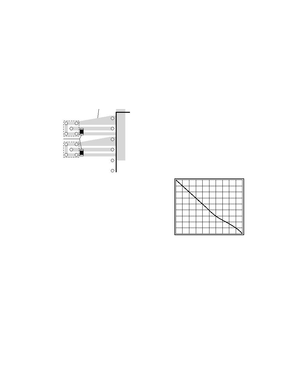
Figure 4: Analog Input Using Guard Ring
Use of the CLC533 with an Analog-to-Digital Converter
To get the most out of the combination of multiplexer and
ADC, a clear understanding of both converter operation
and multiplexer operation is required. Careful attention to
the timing of the convert signal to the ADC and the chan-
nel select signal to the CLC533 is one key to
optimizing performance.
To obtain the best performance from the combination, the
output of the CLC533 must be a valid representation of the
selected input at the time that the ADC samples it. The
time at which the ADC samples the input is determined
by the type of ADC that is being used. Subranging ADCs
usually have a Track-and-Hold (T/H) at their input. For a
successful combination of the multiplexer and the ADC,
the multiplexer timing and the T/H timing must be compati-
ble. When the ADC is given a convert command, the T/H
transitions from Track mode to Hold mode. The delay
between the convert command and this transition is
usually specified as Aperture Delay or as Sampling Time
Offset. To maximize the time that the multiplexer has to
settle and the T/H has to acquire the signal, the multi-
plexer should begin its transition from one input to the
other immediately after the T/H transition has taken
place. However it is during this period of time that a sub-
ranging ADC is performing analog processing of the
sampled signal, and high slew rate transitions on the
input may feed through to the sample being converted.
To minimize this interaction there are two strategies that
can be taken: strategy one applies when the sample rate
of the system is below the rated speed of the converter.
Here the select timing is delayed so that the multiplexer
transition takes place after the A/D has completed one
conversion cycle and is waiting for the next convert
command.
As an example: a CLC935 (15Msps) A/D
converter is being used at 10 MHz, the conversion takes
place in the first 67ns after the convert command, the
next 33ns are spent waiting for the next convert
command and would be an ideal time to transition the
multiplexer from one channel to the next. The second
optimization strategy involves lowering the analog input
slew rate so that it has fewer high frequency components
that might feed through to the hold capacitor while the
converter’s T/H is in hold mode. This slew rate limitation
can be done through the use of the external CLC533
compensation capacitors. Use of this method has the
advantage of limiting some of the excess bandwidth that
the CLC533 has compared to the ADC. This bandwidth
limitation will reduce the amount of high frequency noise
that is aliased back into the sampled band. Figure 5
shows recommended CCOMP values that can be used as
a function of ADC Sample rate. Since the optimal values
will change from one ADC to the next, this graph should
be used as a starting point for CCOMP selection.
Figure 5
Flash ADCs are similar to subranging ADCs in that the
sampling period is very brief. The primary difference is
that the acquisition time of a flash converter is much
shorter than that of a subranging A/D. With a flash ADC
the transition of the mux output should be after the
sampling instant (Aperture delay after the convert
command).
The periods of time during which the
internal circuitry in a flash converter is sensitive to
external disruptions are relatively brief.
It is only
during these points in time that the converter is
susceptible to interference from the input.
It may be
found that a slight delay between the ADC clock and the
CLC533 select lines will have a positive effect on overall
performance.
Channel A
Connector
Channel B
Connector
Pin 1
Chip Resistors
Ground Ring
Recommended CCOMP vs. ADC Sample Rate
Sample Rate (MHz)
C
COMP
(pF)
10
12
14
16
18
20
50
40
30
20
10
相關(guān)PDF資料 |
PDF描述 |
|---|---|
| 5962-9320301MEA | 4-CHANNEL, SGL ENDED MULTIPLEXER, CDIP16 |
| 5962-9320601M2A | 1-CHANNEL POWER SUPPLY SUPPORT CKT, CQCC20 |
| 5962-9320601MEA | 1-CHANNEL POWER SUPPLY SUPPORT CKT, CDIP16 |
| 5962-9320901MPX | DUAL OP-AMP, 2000 uV OFFSET-MAX, CDIP8 |
| 5962-9321501Q2A | STEPPER MOTOR CONTROLLER, 0.5 A, CQCC20 |
相關(guān)代理商/技術(shù)參數(shù) |
參數(shù)描述 |
|---|---|
| 5962-9320401MEA | 功能描述:數(shù)模轉(zhuǎn)換器- DAC 12-BIT DACPORT RoHS:否 制造商:Texas Instruments 轉(zhuǎn)換器數(shù)量:1 DAC 輸出端數(shù)量:1 轉(zhuǎn)換速率:2 MSPs 分辨率:16 bit 接口類型:QSPI, SPI, Serial (3-Wire, Microwire) 穩(wěn)定時(shí)間:1 us 最大工作溫度:+ 85 C 安裝風(fēng)格:SMD/SMT 封裝 / 箱體:SOIC-14 封裝:Tube |
| 5962-9321101MCA | 功能描述:總線接收器 RoHS:否 制造商:Texas Instruments 接收機(jī)數(shù)量:4 接收機(jī)信號(hào)類型:Differential 接口類型:EIA/TIA-422-B, V.11 工作電源電壓:3.3 V 最大工作溫度:+ 85 C 最小工作溫度:- 40 C 封裝 / 箱體:TSSOP-16 封裝:Reel |
| 5962-9321201MPA | 制造商:Linear Technology 功能描述:SMD (STD. MIL DWG.) LT1111MJ8 |
| 5962-9321401MEA | 制造商:Analog Devices 功能描述:V-Ref Programmable 制造商:Analog Devices 功能描述:V-Ref Programmable ±10V 10mA 16-Pin CDIP Tube 制造商:Analog Devices 功能描述:V-REF PROGRAMMABLE 10V 10MA 16CDIP - Rail/Tube 制造商:Analog Devices Inc. 功能描述:Voltage & Current References IC MONO +/-10V REFERENCE 制造商:Analog Devices Inc. 功能描述:IC MONO +/-10V REFERENCE |
| 5962-9321601QPA | 制造商:Texas Instruments 功能描述:OP Amp Single GP 制造商:Rochester Electronics LLC 功能描述:- Bulk |
發(fā)布緊急采購(gòu),3分鐘左右您將得到回復(fù)。