- 您現(xiàn)在的位置:買賣IC網(wǎng) > PDF目錄67328 > 5962-8967402QX (MAXIM INTEGRATED PRODUCTS INC) 1-CH 14-BIT SUCCESSIVE APPROXIMATION ADC, SERIAL/PARALLEL ACCESS, CDIP40 PDF資料下載
參數(shù)資料
| 型號: | 5962-8967402QX |
| 廠商: | MAXIM INTEGRATED PRODUCTS INC |
| 元件分類: | ADC |
| 英文描述: | 1-CH 14-BIT SUCCESSIVE APPROXIMATION ADC, SERIAL/PARALLEL ACCESS, CDIP40 |
| 封裝: | CERAMIC, DIP-40 |
| 文件頁數(shù): | 1/27頁 |
| 文件大小: | 3865K |
| 代理商: | 5962-8967402QX |
當(dāng)前第1頁第2頁第3頁第4頁第5頁第6頁第7頁第8頁第9頁第10頁第11頁第12頁第13頁第14頁第15頁第16頁第17頁第18頁第19頁第20頁第21頁第22頁第23頁第24頁第25頁第26頁第27頁

MAX5713/MAX5714/MAX5715
Ultra-Small, Quad-Channel, 8-/10-/12-Bit Buffered
Output DACs with Internal Reference and SPI Interface
General Description
The MAX5713/MAX5714/MAX5715 4-channel, low-power,
8-/10-/12-bit, voltage-output digital-to-analog converters
(DACs) include output buffers and an internal reference
that is selectable to be 2.048V, 2.500V, or 4.096V. The
MAX5713/MAX5714/MAX5715 accept a wide supply
voltage range of 2.7V to 5.5V with extremely low power
(3mW) consumption to accommodate most low-voltage
applications. A precision external reference input allows
rail-to-rail operation and presents a 100kI (typ) load to
an external reference.
The MAX5713/MAX5714/MAX5715 have a 50MHz 3-wire
SPI/QSPI/MICROWIRE/DSP-compatible serial interface
that also includes a RDY output for daisy-chain applica-
tions. The DAC output is buffered and has a low supply
current of less than 250FA per channel and a low off-
set error of Q0.5mV (typ). On power-up, the MAX5713/
MAX5714/MAX5715 reset the DAC outputs to zero, pro-
viding additional safety for applications that drive valves
or other transducers which need to be off on power-up.
The internal reference is initially powered down to allow
use of an external reference. The MAX5713/MAX5714/
MAX5715 allow simultaneous output updates using soft-
ware LOAD commands or the hardware load DAC logic
input (LDAC).
A clear logic input (CLR) allows the contents of the CODE
and the DAC registers to be cleared asynchronously and
sets the DAC outputs to zero. The MAX5713/MAX5714/
MAX5715 are available in a 14-pin TSSOP and an ultra-
small, 12-bump WLP package and are specified over the
-40NC to +125NC temperature range.
Applications
Programmable Voltage and Current Sources
Gain and Offset Adjustment
Automatic Tuning and Optical Control
Power Amplifier Control and Biasing
Process Control and Servo Loops
Portable Instrumentation
Data Acquisition
Benefits and Features
S
Four High-Accuracy DAC Channels
12-Bit Accuracy Without Adjustment
±1 LSB INL Buffered Voltage Output
Monotonic Over All Operating Conditions
Independent Mode Settings for Each DAC
S
Three Precision Selectable Internal References
2.048V, 2.500V, or 4.096V
S
Internal Output Buffer
Rail-to-Rail Operation with External Reference
4.5s Settling Time
Outputs Directly Drive 2kI Loads
S
Small 5mm x 4.4mm 14-Pin TSSOP or Ultra-Small
1.6mm x 2.2mm 12-Bump WLP Package
S
Wide 2.7V to 5.5V Supply Range
S
Separate 1.8V to 5.5V VDDIO Power-Supply Input
S
50MHz 3-Wire SPI/QSPI/MICROWIRE/DSP
Compatible Serial Interface with RDY Output
S
Power-On-Reset to Zero-Scale DAC Output
S
LDAC and CLR For Asynchronous Control
S
Three Software-Selectable Power-Down Output
Impedances
1kI, 100kI, or High Impedance
19-6394; Rev 3; 6/13
Ordering Information appears at end of data sheet.
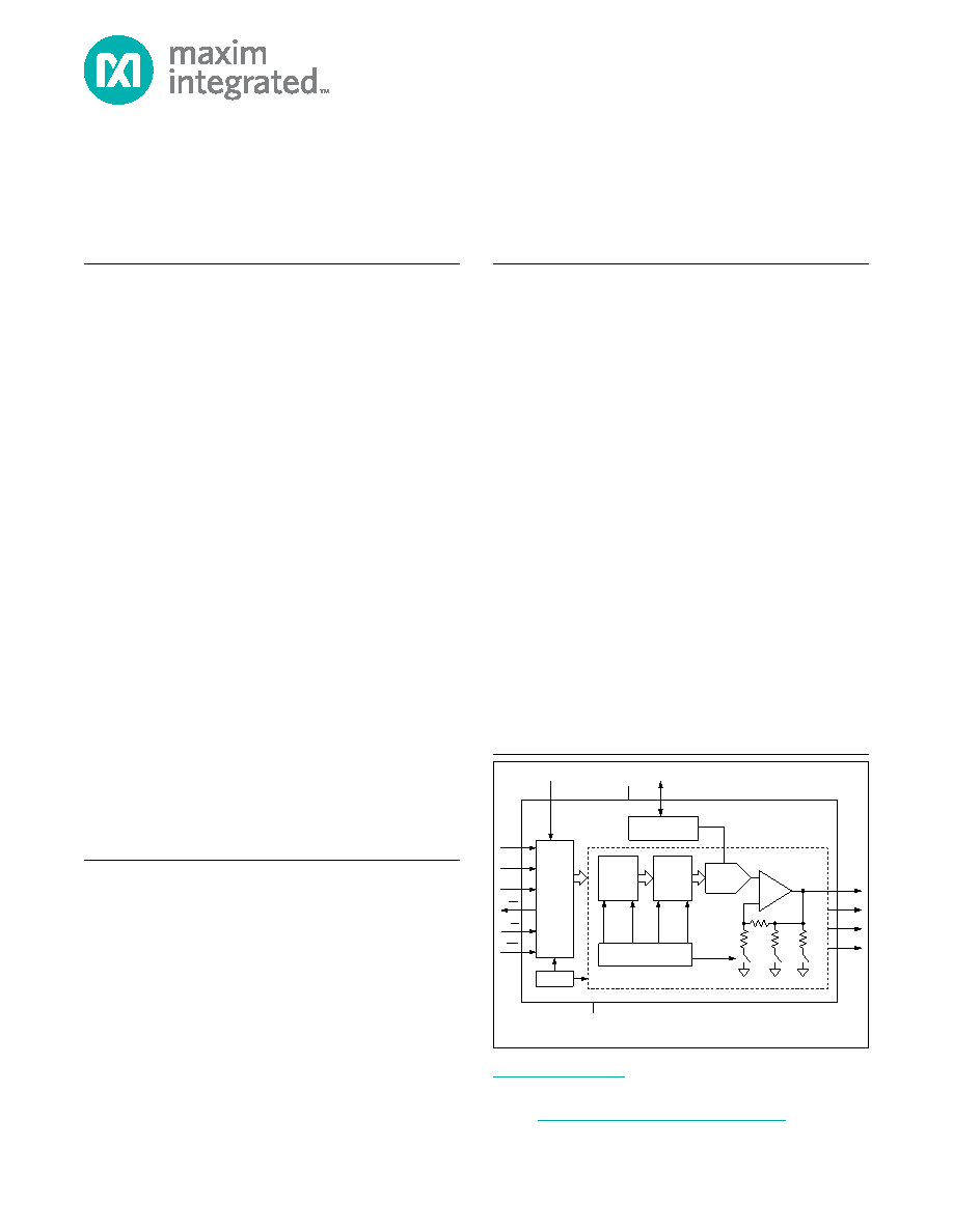
Functional Diagram
QSPI is a trademark of Motorola, Inc.
MICROWIRE is a registered trademark of National
Semiconductor Corporation.
EVALUATION KIT AVAILABLE
DIN
SCLK
CSB
OUTA
BUFFER
POR
VDD
GND
DAC CONTROL LOGIC
POWER-DOWN
REF
OUTB
OUTC
OUTD
VDDIO
(RDY)
CLR
(LDAC)
SPI SERIAL
INTERFACE
( ) TSSOP PACKAGE ONLY
1kI
100kI
CODE
LOAD
CLEAR/
RESET
CLEAR/
RESET
CODE
REGISTER
DAC
LATCH
8-/10-/12-BIT
DAC
1 OF 4 DAC CHANNELS
INTERNAL REFERENCE/
EXTERNAL BUFFER
MAX5713
MAX5714
MAX5715
For pricing, delivery, and ordering information, please contact Maxim Direct
at 1-888-629-4642, or visit Maxim’s website at www.maximintegrated.com.
For related parts and recommended products to use with this part,
refer to: www.maximintegrated.com/MAX5713.related
相關(guān)PDF資料 |
PDF描述 |
|---|---|
| 5962-8967402XX | 1-CH 14-BIT SUCCESSIVE APPROXIMATION ADC, SERIAL/PARALLEL ACCESS, CQCC44 |
| 5962-8967601QX | 1-CH 16-BIT SUCCESSIVE APPROXIMATION ADC, SERIAL/PARALLEL ACCESS, CDIP40 |
| 5962-8967601QX | 1-CH 16-BIT SUCCESSIVE APPROXIMATION ADC, SERIAL/PARALLEL ACCESS, CDIP40 |
| 5962-8967601XX | 1-CH 16-BIT SUCCESSIVE APPROXIMATION ADC, SERIAL/PARALLEL ACCESS, CQCC44 |
| 5962-8967602QX | 1-CH 16-BIT SUCCESSIVE APPROXIMATION ADC, SERIAL/PARALLEL ACCESS, CDIP40 |
相關(guān)代理商/技術(shù)參數(shù) |
參數(shù)描述 |
|---|---|
| 5962-8967701CA | 制造商:Linear Technology 功能描述:AMPLIFIER-OP AMP 制造商:Texas Instruments 功能描述:OP Amp Quad GP ±22V/44V 14-Pin CDIP Tube 制造商:Texas Instruments 功能描述:OP AMP QUAD GP 22V/44V 14CDIP - Rail/Tube 制造商:Texas Instruments 功能描述:LT1014AMJB QUAD PREC OP AMP |
| 5962-8967702CA | 制造商:Texas Instruments 功能描述:OP Amp Quad GP ±22V/44V 14-Pin CDIP Tube 制造商:Texas Instruments 功能描述:OP AMP QUAD GP 22V/44V 14CDIP - Rail/Tube |
| 5962-8967801XA | 制造商:Rochester Electronics LLC 功能描述:- Bulk 制造商:Analog Devices 功能描述: |
| 5962-8967802XA | 制造商:Rochester Electronics LLC 功能描述:8-BIT QUAD MULT DAC IC - Bulk 制造商:Analog Devices 功能描述: |
| 5962-8967901XC | 制造商:SEI 功能描述: |
發(fā)布緊急采購,3分鐘左右您將得到回復(fù)。