- 您現(xiàn)在的位置:買賣IC網(wǎng) > PDF目錄68795 > 5962-8962902LX (ANALOG DEVICES INC) SPECIALTY ANALOG CIRCUIT, CDIP24 PDF資料下載
參數(shù)資料
| 型號: | 5962-8962902LX |
| 廠商: | ANALOG DEVICES INC |
| 元件分類: | 模擬信號調(diào)理 |
| 英文描述: | SPECIALTY ANALOG CIRCUIT, CDIP24 |
| 封裝: | CERDIP-24 |
| 文件頁數(shù): | 7/21頁 |
| 文件大小: | 485K |
| 代理商: | 5962-8962902LX |
AD7569/AD7669
–15–
REV. B
an RD pulse for the AD7569/AD7669. This RD pulse accesses
data from the ADC and places the conversion result into a regis-
ter on the 74646. The rising edge of this pulse generates an in-
terrupt request to the processor. The conversion result is read
from the 74646 register by performing an I/O read to the
decoded address of the 74646. Writing data to the relevant
AD7569/AD7669 DAC involves an I/O write to the 74646,
which transfers the data to the data inputs of the AD7569/
AD7669. Data is latched into the selected DAC register on the
rising edge of IOW.
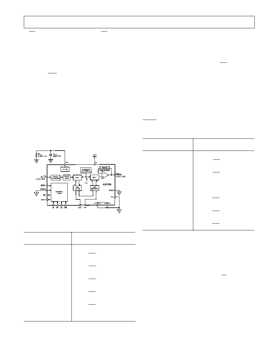
APPLYING THE AD7569/AD7669 DAC
An internal gain/offset network on the AD7569/AD7669 allows
several output voltage ranges. The part can produce unipolar
output ranges of 0 V to +1.25 V or 0 V to +2.5 V and bipolar
output ranges of –1.25 V to +1.25 V or –2.5 V to +2.5 V. Con-
nections for these various output ranges are outlined below.
UNIPOLAR (0 V to +1.25 V) CONFIGURATION
The first of the configurations provides an output voltage range
of 0 V to +1.25 V. This is achieved by tying the VSS and
RANGE inputs to AGNDDAC(= 0 V). Figure 21 shows the con-
figuration of the AD7569 to achieve this output range. A similar
configuration of the AD7669 gives the same output range. The
table for output voltage versus the digital code in the DAC regis-
ter is shown in Table IV.
Figure 21. AD7569 Unipolar (0 V to +1.25 V) Operation
Table IV. Unipolar (0 V to +1.25 V) Code Table
DAC Register Contents
MSB
LSB
Analog Output, VOUT
1111
+VREF
255
256
1000
0001
+VREF
129
256
1000
0000
+VREF
128
256
= +VREF/2
0111
1111
+VREF
127
256
0000
0001
+VREF
1
256
0000
0 V
NOTE: 1 LSB = (VREF) (2
–8) = V
REF (1/256); VREF = +1.25 V Nominal
UNIPOLAR (0 V to +2.5 V) CONFIGURATION
The 0 V to +2.5 V output voltage range is achieved by tying VSS
to AGNDDAC(= 0 V) and the RANGE input to VDD. The table
for output voltage versus digital code is as in Table IV with
2.VREF replacing VREF. Note that for this range
1 LSB
= 2.V
REF (2
8 ) = V
REF
1
128
BIPOLAR (–1.25 V to +1.25 V) CONFIGURATION
The first of the bipolar configurations is achieved by tying the
RANGE input to AGNDDAC(= 0 V) and VSS to –5 V. The VSS
voltage level at which the AD7569/AD7669 changes to bipolar
operation is approximately –1 V. When the part is configured
for bipolar outputs, the input coding becomes twos comple-
ment. The table for output voltage versus the digital code in the
DAC register is shown in Table V. Note as with the unipolar
configuration, a digital input code of all 0s produces an output
of 0 V. It should be noted, however, that a low pulse on the
RESET
line for the bipolar ranges sets the output voltage to
negative full scale.
Table V. Bipolar (–1.25 V to +1.25 V) Code Table
DAC Register Contents
MSB
LSB
Analog Output, VOUT
0111
1111
+VREF
127
128
0000
0001
+VREF
1
128
0000
0 V
1111
–VREF
1
128
1000
0001
–VREF
127
128
1000
0000
–VREF
128
= –VREF
NOTE: 1 LSB = (VREF)(2
–7) = V
REF (1/128)
BIPOLAR (–2.5 V to +2.5 V) CONFIGURATION
The –2.5 V to +2.5 V bipolar output range is achieved by tying
the RANGE input to VDD and the VSS input to –5 V. Once
again, the input coding is 2s complement. The table for output
voltage versus digital code is as in Table V with 2.VREF replacing
VREF. Note that for this range
1 LSB
= 4.V
REF (2
8 ) = V
REF
1
64
相關(guān)PDF資料 |
PDF描述 |
|---|---|
| 5962-8963401CA | QUAD OP-AMP, 2500 uV OFFSET-MAX, 34 MHz BAND WIDTH, CDIP14 |
| 5962-8963401CX | QUAD OP-AMP, 2500 uV OFFSET-MAX, 34 MHz BAND WIDTH, CDIP14 |
| 5962-89635012X | OP-AMP, 3000 uV OFFSET-MAX, 10 MHz BAND WIDTH, CQCC20 |
| 5962-8963501PX | OP-AMP, 3000 uV OFFSET-MAX, 10 MHz BAND WIDTH, CDIP8 |
| 5962-8964301XC | OP-AMP, 10000 uV OFFSET-MAX, 40 MHz BAND WIDTH, MBCY12 |
相關(guān)代理商/技術(shù)參數(shù) |
參數(shù)描述 |
|---|---|
| 5962-8963001EA | 制造商:National Semiconductor Corporation 功能描述:Dual Receiver RS-232/RS-422/RS-423 16-Pin CDIP Rail 制造商:National Semiconductor 功能描述:Dual Receiver RS-232/RS-422/RS-423 16-Pin CDIP Rail |
| 5962-8963101PA | 制造商:Rochester Electronics LLC 功能描述:- Bulk |
| 5962-8963201PA | 制造商:Rochester Electronics LLC 功能描述:SMD HA7-5112 DUAL LOW NOISE OP AMP 8 LD CDIP - Bulk |
| 5962-89635012A | 制造商:Intersil Corporation 功能描述:OP AMP SGL GP 15V 20CLCC - Rail/Tube |
| 5962-8963501PA | 制造商:Intersil Corporation 功能描述:SMD VERSIO HA7-5101/883 NOT DUAL MARKED - Rail/Tube |
發(fā)布緊急采購,3分鐘左右您將得到回復(fù)。