- 您現(xiàn)在的位置:買賣IC網(wǎng) > PDF目錄67327 > 5962-89616032X (MAXIM INTEGRATED PRODUCTS INC) 1-CH 8-BIT SUCCESSIVE APPROXIMATION ADC, PARALLEL ACCESS, CQCC20 PDF資料下載
參數(shù)資料
| 型號(hào): | 5962-89616032X |
| 廠商: | MAXIM INTEGRATED PRODUCTS INC |
| 元件分類: | ADC |
| 英文描述: | 1-CH 8-BIT SUCCESSIVE APPROXIMATION ADC, PARALLEL ACCESS, CQCC20 |
| 封裝: | QCC-20 |
| 文件頁(yè)數(shù): | 11/12頁(yè) |
| 文件大小: | 238K |
| 代理商: | 5962-89616032X |
MAX541/MAX542
+5V, Serial-Input, Voltage-Output, 16-Bit DACs
8
_______________________________________________________________________________________
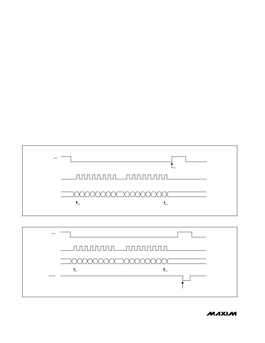
Digital Interface
The MAX541/MAX542’s digital interface is a standard
3-wire connection compatible with SPI/QSPI/
MICROWIRE interfaces. The chip-select input (CS)
frames the serial data loading at the data-input pin
(DIN). Immediately following CS’s high-to-low transition,
the data is shifted synchronously and latched into the
input register on the rising edge of the serial clock input
(SCLK). After 16 data bits have been loaded into the
serial input register, it transfers its contents to the DAC
latch on CS’s low-to-high transition (Figure 3a). Note
that if CS is not kept low during the entire 16 SCLK
cycles, data will be corrupted. In this case, reload the
DAC latch with a new 16-bit word.
Alternatively, for the MAX542, LDAC allows the DAC
latch to update asynchronously by pulling LDAC low
after CS goes high (Figure 3b). Hold LDAC high during
the data-loading sequence.
External Reference
The MAX541/MAX542 operate with external voltage ref-
erences from 2V to 3V. The reference voltage deter-
mines the DAC’s full-scale output voltage. Kelvin
connections are provided with the MAX542 for optimum
performance.
Power-On Reset
The MAX541/MAX542 have a power-on reset circuit to
set the DAC’s output to 0V in unipolar mode when VDD
is first applied. This ensures that unwanted DAC output
voltages will not occur immediately following a system
power-up, such as after a loss of power. In bipolar
mode, the DAC output is set to -VREF.
;
;;
CS
SCLK
DIN
MSB
LSB
D15
D8
D7 D6 D5 D4 D3 D2
D1 D0
DAC
UPDATED
D14 D13 D12 D11 D10 D9
;
;; ;;;
CS
SCLK
DIN
LDAC
MSB
LSB
D15 D14 D13 D12 D11 D10 D9 D8
D7 D6 D5 D4 D3 D2 D1
D0
DAC
UPDATED
Figure 3a. MAX541/MAX542 3-Wire Interface Timing Diagram (LDAC = DGND for MAX542)
Figure 3b. MAX542 4-Wire Interface Timing Diagram
相關(guān)PDF資料 |
PDF描述 |
|---|---|
| 5962-89616042X | 1-CH 8-BIT SUCCESSIVE APPROXIMATION ADC, PARALLEL ACCESS, CQCC20 |
| DS1668 | 1 TIMER(S), REAL TIME CLOCK, PDIP28 |
| 5962-8961603VX | 1-CH 8-BIT SUCCESSIVE APPROXIMATION ADC, PARALLEL ACCESS, CDIP18 |
| 5962-8961604VX | 1-CH 8-BIT SUCCESSIVE APPROXIMATION ADC, PARALLEL ACCESS, CDIP18 |
| 5962-8962001PA | 1 CHANNEL, VIDEO AMPLIFIER, CDIP8 |
相關(guān)代理商/技術(shù)參數(shù) |
參數(shù)描述 |
|---|---|
| 5962-8961603VA | 功能描述:模數(shù)轉(zhuǎn)換器 - ADC RoHS:否 制造商:Texas Instruments 通道數(shù)量:2 結(jié)構(gòu):Sigma-Delta 轉(zhuǎn)換速率:125 SPs to 8 KSPs 分辨率:24 bit 輸入類型:Differential 信噪比:107 dB 接口類型:SPI 工作電源電壓:1.7 V to 3.6 V, 2.7 V to 5.25 V 最大工作溫度:+ 85 C 安裝風(fēng)格:SMD/SMT 封裝 / 箱體:VQFN-32 |
| 5962-89616042A | 制造商:Rochester Electronics LLC 功能描述:- Bulk |
| 5962-89616042C | 功能描述:模數(shù)轉(zhuǎn)換器 - ADC CMOS 8-Bit Microprocessor Compatible ADC RoHS:否 制造商:Texas Instruments 通道數(shù)量:2 結(jié)構(gòu):Sigma-Delta 轉(zhuǎn)換速率:125 SPs to 8 KSPs 分辨率:24 bit 輸入類型:Differential 信噪比:107 dB 接口類型:SPI 工作電源電壓:1.7 V to 3.6 V, 2.7 V to 5.25 V 最大工作溫度:+ 85 C 安裝風(fēng)格:SMD/SMT 封裝 / 箱體:VQFN-32 |
| 5962-8961604VA | 功能描述:模數(shù)轉(zhuǎn)換器 - ADC RoHS:否 制造商:Texas Instruments 通道數(shù)量:2 結(jié)構(gòu):Sigma-Delta 轉(zhuǎn)換速率:125 SPs to 8 KSPs 分辨率:24 bit 輸入類型:Differential 信噪比:107 dB 接口類型:SPI 工作電源電壓:1.7 V to 3.6 V, 2.7 V to 5.25 V 最大工作溫度:+ 85 C 安裝風(fēng)格:SMD/SMT 封裝 / 箱體:VQFN-32 |
| 5962-8961701LA | 功能描述:數(shù)模轉(zhuǎn)換器- DAC IC MONO 12-BIT DAC IC RoHS:否 制造商:Texas Instruments 轉(zhuǎn)換器數(shù)量:1 DAC 輸出端數(shù)量:1 轉(zhuǎn)換速率:2 MSPs 分辨率:16 bit 接口類型:QSPI, SPI, Serial (3-Wire, Microwire) 穩(wěn)定時(shí)間:1 us 最大工作溫度:+ 85 C 安裝風(fēng)格:SMD/SMT 封裝 / 箱體:SOIC-14 封裝:Tube |
發(fā)布緊急采購(gòu),3分鐘左右您將得到回復(fù)。