- 您現(xiàn)在的位置:買賣IC網(wǎng) > PDF目錄56729 > 5962-8948102VX (ANALOG DEVICES INC) PARALLEL, WORD INPUT LOADING, 0.6 us SETTLING TIME, 12-BIT DAC, CDIP18 PDF資料下載
參數(shù)資料
| 型號: | 5962-8948102VX |
| 廠商: | ANALOG DEVICES INC |
| 元件分類: | DAC |
| 英文描述: | PARALLEL, WORD INPUT LOADING, 0.6 us SETTLING TIME, 12-BIT DAC, CDIP18 |
| 封裝: | GLASS SEALED, CERDIP-18 |
| 文件頁數(shù): | 5/9頁 |
| 文件大?。?/td> | 206K |
| 代理商: | 5962-8948102VX |
AD7541A
–5–
REV. B
BIPOLAR OPERATION
(4-QUADRANT MULTIPLICATION)
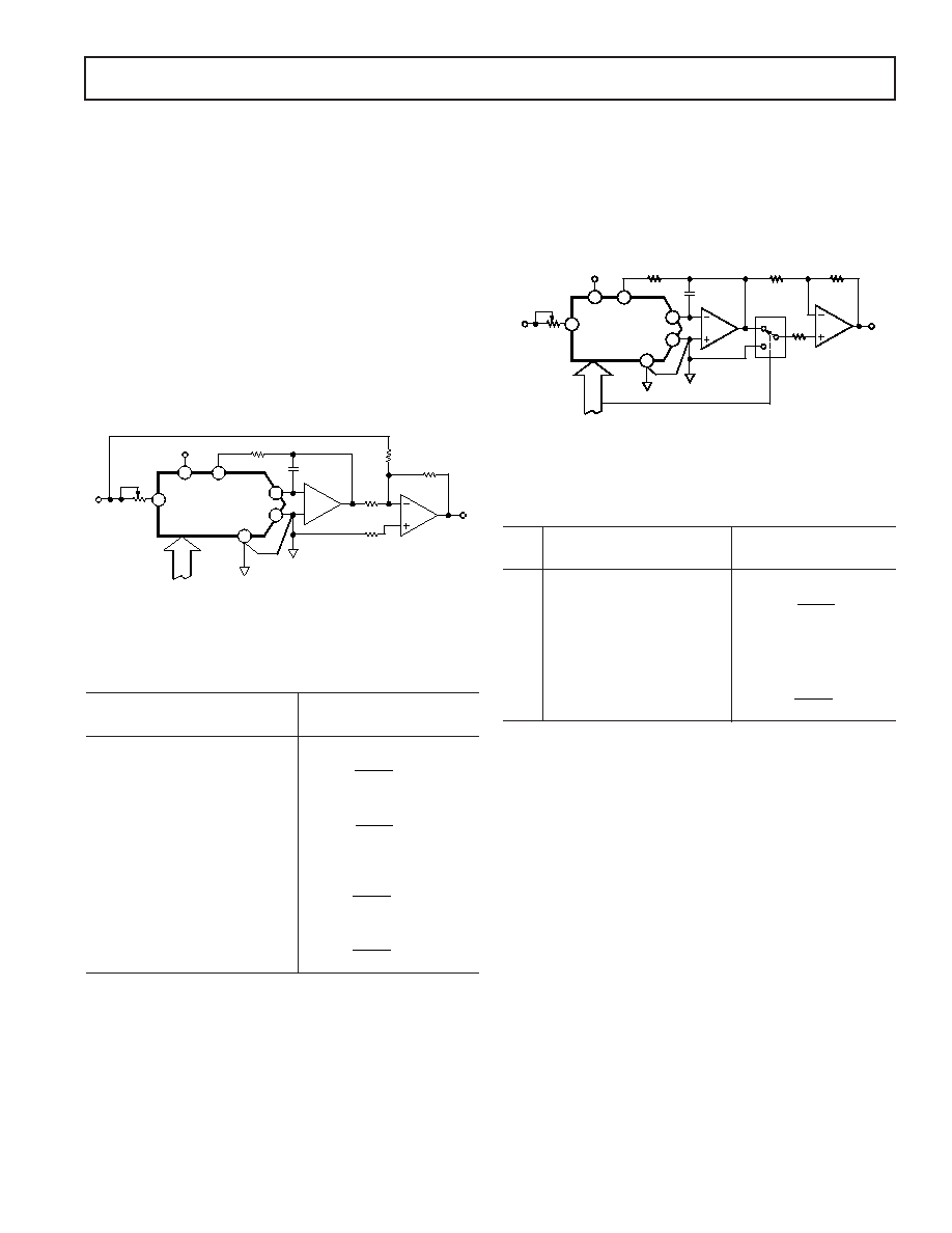
Figure 5 and Table III illustrate the circuitry and code relation-
ship for bipolar operation. With a dc reference (positive or nega-
tive polarity) the circuit provides offset binary operation. With
an ac reference the circuit provides full 4-quadrant multiplication.
With the DAC loaded to 1000 0000 0000, adjust R1 for
VOUT = 0 V (alternatively, one can omit R1 and R2 and adjust
the ratio of R3 to R4 for VOUT = 0 V). Full-scale trimming can
be accomplished by adjusting the amplitude of VREF or by vary-
ing the value of R5.
As in unipolar operation, A1 must be chosen for low VOS and
low IB. R3, R4 and R5 must be selected for matching and track-
ing. Mismatch of 2R3 to R4 causes both offset and full-scale
error. Mismatch of R5 to R4 or 2R3 causes full-scale error. C1
phase compensation (10 pF to 50 pF) may be required for sta-
bility, depending on amplifier used.
AD7541A
A1
3
R2
*
VDD
16
17
18
1
2
VDD
RFB
VREF
PINS 4–15
GND
OUT1
OUT2
R1
*
VIN
BIT 1 – BIT 12
DIGITAL
GROUND
ANALOG
COMMON
C1
33pF
AD544L
VOUT
AD544J
A2
R4
20k
R5
20k
R3
10k
R6
5k
10%
*FOR VALUES OF R1 AND R2
SEE TABLE 1.
Figure 5. Bipolar Operation (4-Quadrant Multiplication)
Table III. Bipolar Code Table for Offset Binary Circuit of
Figure 5
Binary Number in DAC
MSB
LSB
Analog Output, VOUT
1 1 1 1
+VIN
2047
2048
1 0 0 0
0 0 0 0
0 0 0 1
+VIN
1
2048
1 0 0 0
0 0 0 0
0 Volts
0 1 1 1
1 1 1 1
–VIN
1
2048
0 0 0 0
–VIN
2048
Figure 6 and Table IV show an alternative method of achieving
bipolar output. The circuit operates with sign plus magnitude
code and has the advantage of giving 12-bit resolution in each
quadrant, compared with 11-bit resolution per quadrant for the
circuit of Figure 5. The AD7592 is a fully protected CMOS
changeover switch with data latches. R4 and R5 should match
each other to 0.01% to maintain the accuracy of the D/A con-
verter. Mismatch between R4 and R5 introduces a gain error.
A2
AD7541A
A1
3
R2
*
VDD
16
17
18
1
2
VDD
RFB
VREF
PINS 4–15
GND
OUT1
OUT2
R1
*
VIN
BIT 1 – BIT 12
DIGITAL
GROUND
ANALOG
COMMON
C1
33pF
AD544L
VOUT
AD544J
R5
20k
*FOR VALUES OF R1 AND R2
SEE TABLE 1.
R4
20k
R3
10k
10%
1/2 AD7592JN
SIGN BIT
Figure 6. 12-Bit Plus Sign Magnitude Operation
Table IV. 12-Bit Plus Sign Magnitude Code Table for Circuit
of Figure 6
Sign
Binary Number in DAC
Bit
MSB
LSB
Analog Output, VOUT
0
1 1 1 1
+VIN
×
4095
4096
0
0 0 0 0
0 Volts
1
0 0 0 0
0 Volts
1
1 1 1 1 1 1 1 1
1 1 1 1
–VIN ×
4095
4096
Note: Sign bit of “0” connects R3 to GND.
相關PDF資料 |
PDF描述 |
|---|---|
| 5962-8949907XC | SYNCHRO OR RESOLVER TO DIGITAL CONVERTER, DIP36 |
| 5962-8949908XC | SYNCHRO OR RESOLVER TO DIGITAL CONVERTER, DIP36 |
| 5962-8990812XC | SYNCHRO OR RESOLVER TO DIGITAL CONVERTER, DIP36 |
| 5962-8990813XC | SYNCHRO OR RESOLVER TO DIGITAL CONVERTER, DIP36 |
| 5962-8990811XC | SYNCHRO OR RESOLVER TO DIGITAL CONVERTER, DIP36 |
相關代理商/技術參數(shù) |
參數(shù)描述 |
|---|---|
| 5962-89481032A | 制造商:Rochester Electronics LLC 功能描述:- Bulk |
| 5962-8948103VA | 制造商:Rochester Electronics LLC 功能描述:- Bulk |
| 5962-8948104VA | 制造商:Rochester Electronics LLC 功能描述:12-BIT MULTIPLYING DAC IC - Bulk |
| 5962-8948401M3A | 制造商:QP Semiconductor 功能描述:EPROM UV 64K-Bit 8K x 8 50ns 28-Pin LLCC |
| 5962-8948403MXA | 制造商:QP Semiconductor 功能描述:EPROM UV 64K-Bit 8K x 8 15ns 28-Pin CDIP |
發(fā)布緊急采購,3分鐘左右您將得到回復。