- 您現(xiàn)在的位置:買賣IC網(wǎng) > PDF目錄157276 > 5962-8766001GA (MAXIM INTEGRATED PRODUCTS INC) 2 CHANNEL, BUF OR INV BASED MOSFET DRIVER, MBCY8 PDF資料下載
參數(shù)資料
| 型號(hào): | 5962-8766001GA |
| 廠商: | MAXIM INTEGRATED PRODUCTS INC |
| 元件分類: | MOSFETs |
| 英文描述: | 2 CHANNEL, BUF OR INV BASED MOSFET DRIVER, MBCY8 |
| 封裝: | METAL CAN-8 |
| 文件頁數(shù): | 8/15頁 |
| 文件大小: | 784K |
| 代理商: | 5962-8766001GA |
MAX706P/R/S/T
,MAX706AP/AR/AS/A
T
,MAX708R/S/T
+3V Voltage Monitoring, Low-Cost P
Supervisory Circuits
2
_______________________________________________________________________________________
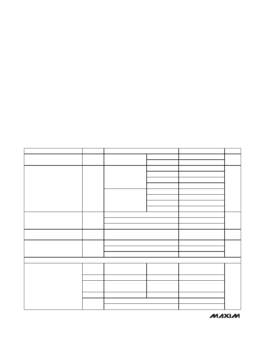
ABSOLUTE MAXIMUM RATINGS
ELECTRICAL CHARACTERISTICS
(MAX70_P/R, MAX706AP/AR: VCC = 2.7V to 5.5V; MAX70_S, MAX706AS: VCC = 3.0V to 5.5V; MAX70_T, MAX706AT: VCC = 3.15V to
5.5V; TJ = TA = TMIN to TMAX, unless otherwise noted. Typical values are at TJ = TA = +25
°C.) (Note 2)
Stresses beyond those listed under “Absolute Maximum Ratings” may cause permanent damage to the device. These are stress ratings only, and functional
operation of the device at these or any other conditions beyond those indicated in the operational sections of the specifications is not implied. Exposure to
absolute maximum rating conditions for extended periods may affect device reliability.
Terminal Voltage (with respect to GND)
VCC ........................................................................-0.3V to +6V
All Other Inputs (Note 1)..........................-0.3V to (VCC + 0.3V)
Input Current
VCC ..................................................................................20mA
GND .................................................................................20mA
Output Current (all outputs) ................................................20mA
Continuous Power Dissipation (TA = +70
°C)
8-Pin CERDIP (derate 8mW/
°C above +70°C)..............640mW
8-Pin PDIP (derate 9.1mW/
°C above +70°C).............727.3mW
8-Pin SO (derate 5.9mW/
°C above +70°C)................470.6mW
8-Pin MAX (derate 4.5mW/oC above +70
°C)..............362mW
Operating Temperature Range
MAX70_C .............................................................0
°C to +70°C
MAX70_E ..........................................................-40
°C to +85°C
MAX70_M .......................................................-55
°C to +125°C
Junction Temperature ......................................................+150
°C
Storage Temperature Range .............................-65
°C to +150°C
Lead Temperature (soldering, 10s) .................................+300
°C
Note 1: The input-voltage limits on PFI, WDI, and MR can be exceeded if the input current is less than 10mA.
PARAMETER
SYMBOL
CONDITIONS
MIN
TYP
MAX
UNITS
MAX70_C
1.0
5.5
Supply Voltage Range
VCC
MAX70_E/M
1.2
5.5
V
MAX706_C
90
200
MAX706_E/M
90
300
MAX708_C
50
200
VCC < 3.6V
MAX708_E/M
50
300
MAX706_C
135
350
MAX706_E/M
135
500
MAX708_C
65
350
Supply Current
ISUPPLY
VCC < 5.5V
MAX708_E/M
65
500
A
MAX70_P/R, MAX706AP/AR
2.55
2.63
2.70
MAX70_S, MAX706AS
2.85
2.93
3.00
Reset Threshold (Note 3)
(VCC Falling)
VRST
MAX70_T, MAX706AT
3.00
3.08
3.15
V
Reset Threshold Hysteresis
(Note 3)
VHYS
20
mV
MAX70_P/R, MAX706AP/AR VCC = 3.0V
140
200
280
MAX70_S, MAX706AS, VCC = 3.3V
140
200
280
Reset Pulse Width (Note 3)
tRST
VCC = 5V
200
ms
RESET OUTPUT
VOH
VRST(MAX) < VCC < 3.6V ISOURCE = 500A
0.8 x
VCC
VOL
VRST(MAX) < VCC < 3.6V ISINK = 1.2mA
0.3
VOH
4.5V < VCC < 5.5V
IRSOURCE =
800A
VCC -
1.5
VOL
4.5V < VCC < 5.5V
ISINK = 3.2mA
0.4
MAX70_C VCC = 1.0V, ISINK = 50A
0.3
Output-Voltage High
(MAX70_R/S/T)
(MAX706AR/AS/AT)
VOL
MAX70_E/M: VCC = 1.2V, ISINK = 100A
0.3
V
相關(guān)PDF資料 |
PDF描述 |
|---|---|
| 5962-8768901VA | 8-CHANNEL, SGL ENDED MULTIPLEXER, CDIP18 |
| 5962-8770804UX | 12-BIT, MICROPROGRAM SEQUENCER, CQCC44 |
| 5962-8773503XX | 24-BIT, 32.768 MHz, OTHER DSP, CPGA100 |
| 5962-8850103ZA | 16-BIT, 20 MHz, MICROPROCESSOR, CPGA68 |
| 5962-8850602XA | MULTIFUNCTION PERIPHERAL, CDIP48 |
相關(guān)代理商/技術(shù)參數(shù) |
參數(shù)描述 |
|---|---|
| 5962-8766001PA | 功能描述:功率驅(qū)動(dòng)器IC Dual-Power MOSFET Driver RoHS:否 制造商:Micrel 產(chǎn)品:MOSFET Gate Drivers 類型:Low Cost High or Low Side MOSFET Driver 上升時(shí)間: 下降時(shí)間: 電源電壓-最大:30 V 電源電壓-最小:2.75 V 電源電流: 最大功率耗散: 最大工作溫度:+ 85 C 安裝風(fēng)格:SMD/SMT 封裝 / 箱體:SOIC-8 封裝:Tube |
| 5962-8766107XA | 制造商:e2v 功能描述:EPROM UV 128K-Bit 16K x 8 300ns 28-Pin CDIP 制造商:e2v technologies 功能描述:EPROM UV 128K-Bit 16K x 8 300ns 28-Pin CDIP |
| 59628766201EA | 制造商:Advanced Micro Devices 功能描述: |
| 5962-87663012A | 制造商:QP Semiconductor 功能描述:Bus XCVR Single 8-CH 3-ST 20-Pin CLLCC |
| 5962-8766301BSA | 制造商:QP Semiconductor 功能描述:ACT245 NSC DIE - FP |
發(fā)布緊急采購,3分鐘左右您將得到回復(fù)。