- 您現(xiàn)在的位置:買賣IC網(wǎng) > PDF目錄67323 > 5962-8670401VPA (TEXAS INSTRUMENTS INC) 1 A SWITCHING CONTROLLER, 500 kHz SWITCHING FREQ-MAX, CDIP8 PDF資料下載
參數(shù)資料
| 型號: | 5962-8670401VPA |
| 廠商: | TEXAS INSTRUMENTS INC |
| 元件分類: | 穩(wěn)壓器 |
| 英文描述: | 1 A SWITCHING CONTROLLER, 500 kHz SWITCHING FREQ-MAX, CDIP8 |
| 封裝: | CERAMIC, DIP-8 |
| 文件頁數(shù): | 23/33頁 |
| 文件大小: | 1361K |
| 代理商: | 5962-8670401VPA |
第1頁第2頁第3頁第4頁第5頁第6頁第7頁第8頁第9頁第10頁第11頁第12頁第13頁第14頁第15頁第16頁第17頁第18頁第19頁第20頁第21頁第22頁當(dāng)前第23頁第24頁第25頁第26頁第27頁第28頁第29頁第30頁第31頁第32頁第33頁
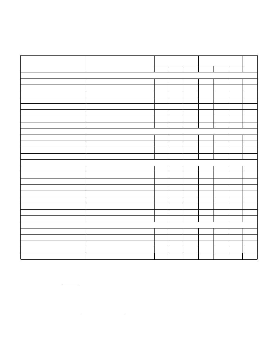
3
PARAMETER
TEST CONDITIONS
UC1842/3/4/5
UC2842/3/4/5
UC3842/3/4/5
UNITS
MIN
TYP
MAX
MIN
TYP
MAX
Reference Section
Output Voltage
TJ = 25°C, IO = 1mA
4.95
5.00
5.05
4.90
5.00
5.10
V
Line Regulation
12
≤ VIN ≤ 25V
6
20
6
20
mV
Load Regulation
1
≤ I0 ≤ 20mA
6
25
6
25
mV
Temp. Stability
(Note 2) (Note 7)
0.2
0.4
0.2
0.4
mV/°C
Total Output Variation
Line, Load, Temp. (Note 2)
4.9
5.1
4.82
5.18
V
Output Noise Voltage
10Hz
≤ f ≤ 10kHz, TJ = 25°C (Note2)
50
V
Long Term Stability
TA = 125°C, 1000Hrs. (Note 2)
5
25
5
25
mV
Output Short Circuit
-30
-100
-180
-30
-100
-180
mA
Oscillator Section
Initial Accuracy
TJ = 25°C (Note 6)
47
52
57
47
52
57
kHz
Voltage Stability
12
≤ VCC ≤ 25V
0.2
1
0.2
1
%
Temp. Stability
TMIN
≤ TA ≤ TMAX (Note 2)
5
%
Amplitude
VPIN 4 peak to peak (Note 2)
1.7
V
Error Amp Section
Input Voltage
VPIN 1 = 2.5V
2.45
2.50
2.55
2.42
2.50
2.58
V
Input Bias Current
-0.3
-1
-0.3
-2
A
AVOL
2
≤ VO ≤ 4V
65
90
65
90
dB
Unity Gain Bandwidth
(Note 2) TJ = 25°C
0.7
1
0.7
1
MHz
PSRR
12
≤ VCC ≤ 25V
60
70
60
70
dB
Output Sink Current
VPIN 2 = 2.7V, VPIN 1 = 1.1V
2
6
2
6
mA
Output Source Current
VPIN 2 = 2.3V, VPIN 1 = 5V
-0.5
-0.8
-0.5
-0.8
mA
VOUT High
VPIN 2 = 2.3V, RL = 15k to ground
5
6
5
6
V
VOUT Low
VPIN 2 = 2.7V, RL = 15k to Pin 8
0.7
1.1
0.7
1.1
V
Current Sense Section
Gain
(Notes 3 and 4)
2.85
3
3.15
2.85
3
3.15
V/V
Maximum Input Signal
VPIN 1 = 5V (Note 3)
0.9
1
1.1
0.9
1
1.1
V
PSRR
12
≤ VCC ≤ 25V (Note 3) (Note 2)
70
dB
Input Bias Current
-2
-10
-2
-10
A
Delay to Output
VPIN 3 = 0 to 2V (Note 2)
150
300
150
300
ns
UC1842/3/4/5
UC2842/3/4/5
UC3842/3/4/5
ELECTRICAL CHARACTERISTICS:
Unless otherwise stated, these specifications apply for -55°C
≤ TA ≤ 125°C for the
UC184X; -40°C
≤ TA ≤ 85°C for the UC284X; 0°C ≤ TA ≤ 70°C for the 384X; VCC = 15V
(Note 5); RT = 10k; CT = 3.3nF, TA=TJ.
Note 2:
These parameters, although guaranteed, are not 100% tested in production.
Note 3:
Parameter measured at trip point of latch with VPIN 2 =0.
Note 4:
Gain defined as
A
VPIN
V
=≤
≤
1
3
03 0 8
,.
Note 5:
Adjust VCC above the start threshold before setting at 15V.
Note 6:
Output frequency equals oscillator frequency for the UC1842 and UC1843.
Output frequency is one half oscillator frequency for the UC1844 and UC1845.
Note 7:
Temperature stability, sometimes referred to as average temperature coefficient, is described by the equation:
Temp Stability V
max
VREF min
TJ max
TJ min
REF
=
()
(
)
()
(
)
VREF (max) and VREF (min) are the maximum and minimum reference voltages measured over the appropriate
temperature range. Note that the extremes in voltage do not necessarily occur at the extremes in temperature.
相關(guān)PDF資料 |
PDF描述 |
|---|---|
| 5962-8670403VPA | 1 A SWITCHING CONTROLLER, 500 kHz SWITCHING FREQ-MAX, CDIP8 |
| 5962-8670404VXA | 1 A SWITCHING CONTROLLER, 500 kHz SWITCHING FREQ-MAX, CQCC20 |
| 5962-8670403VXA | 1 A SWITCHING CONTROLLER, 500 kHz SWITCHING FREQ-MAX, CQCC20 |
| 5962-8670402VXA | 1 A SWITCHING CONTROLLER, 500 kHz SWITCHING FREQ-MAX, CQCC20 |
| 5962-8670401XA | 1 A SWITCHING CONTROLLER, 500 kHz SWITCHING FREQ-MAX, CQCC20 |
相關(guān)代理商/技術(shù)參數(shù) |
參數(shù)描述 |
|---|---|
| 5962-8670402DA | 制造商:Texas Instruments 功能描述:CURRENT MODE PWM CNTRLR 1A 14CFPAK - Rail/Tube |
| 5962-8670402PA | 制造商:Texas Instruments 功能描述:CURRENT MODE PWM CNTRLR 1A 8CDIP - Rail/Tube |
| 5962-8670402V2A | 制造商:Texas Instruments 功能描述:CURRENT MODE PWM CNTRLR 1A 20LCCC - Rail/Tube |
| 5962-8670402VPA | 制造商:Texas Instruments 功能描述:Current Mode PWM Controller 1A 8-Pin CDIP |
| 5962-8670402XA | 制造商:Texas Instruments 功能描述:5962-8670402XA, CUR MODE PWM CONT - Rail/Tube |
發(fā)布緊急采購,3分鐘左右您將得到回復(fù)。