- 您現(xiàn)在的位置:買(mǎi)賣(mài)IC網(wǎng) > PDF目錄63392 > 5962-0520901KXC 64-CHANNEL, SGL ENDED MULTIPLEXER, CQFP96 PDF資料下載
參數(shù)資料
| 型號(hào): | 5962-0520901KXC |
| 元件分類: | 多路復(fù)用及模擬開(kāi)關(guān) |
| 英文描述: | 64-CHANNEL, SGL ENDED MULTIPLEXER, CQFP96 |
| 封裝: | 1.320 X 1.320 INCH, 0.200 INCH HEIGHT, HERMETIC SEALED, CERAMIC, QFP-96 |
| 文件頁(yè)數(shù): | 5/10頁(yè) |
| 文件大?。?/td> | 111K |
| 代理商: | 5962-0520901KXC |
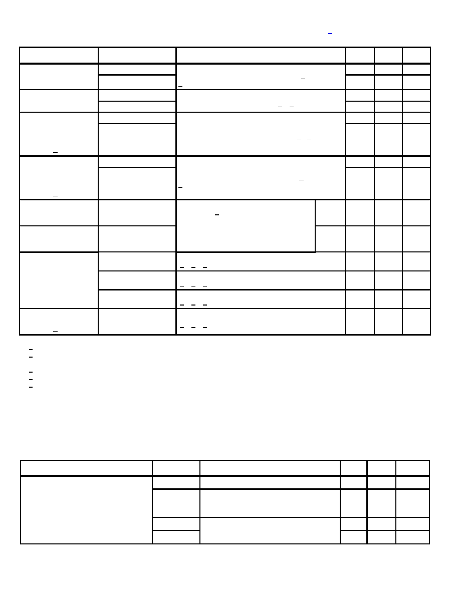
4
SCD8504 Rev E 9/29/08
Aeroflex Plainview
d
Positive Input
Leakage Current
CH0-CH63
+ISOFFOUTPUT(ALL)VIN = +10V, VEN = 4V, output and all
unused MUX inputs under test = -10V
2/,
3/
-100
+700
nA
+ISOFFCURRENT(ALL)
-100
+700
nA
Negative Input Leakage
Current CH0-CH63
-ISOFFOUTPUT(ALL)
VIN = -10V, VEN = 4V, output and all unused
MUX inputs under test = +10V 2/, 3/
-100
+700
nA
-ISOFFCURRENT(ALL)
-100
+700
nA
Output Leakage
Current OUTPUTS
(pins 25, 26, 68 & 70)
Mux Monitor
(pin 69)
6/
+IDOFFOUTPUT(ALL)
VOUT = +10V, VEN = 4V, output and all
unused MUX inputs under test = -10V 3/, 4/
-100
+100
nA
+IDOFFCURRENT(ALL)
-100
+100
nA
Output Leakage
Current OUTPUTS
(pins 25, 26, 68 & 70)
Mux Monitor
(pin 69)
6/
-IDOFFOUTPUT(ALL)
VOUT = -10V, VEN = 4V, output and all
unused MUX inputs under test = +10V 3/,
4/
-100
+100
nA
-IDOFFCURRENT(ALL)
-100
+100
nA
Input Clamped Voltage
CH0 - CH63
+VCLMP(0-63)
VEN = 4V, all unused MUX inputs under test
are open.
3/
+25°C
+125°C
-55°C
18.0
17.5
23.0
23.5
22.5
V
Input Clamped Voltage
CH0 - CH63
-VCLMP(0-63)
+25°C
+125°C
-55°C
-23.0
-23.5
-22.5
-18.0
-17.5
V
Switch ON Resistance
OUTPUTS
(pins 25, 26, 68 & 70)
RDS(ON)(0-63)
A
VIN = +15V, VEN = 0.8V, IOUT = -1mA
2/, 3/, 5/
500
3000
Ω
RDS(ON)(0-63)
B
VIN = +5V, VEN = 0.8V, IOUT = -1mA
2/, 3/, 5/
500
3000
Ω
RDS(ON)(0-63)
C
VIN = -5V, VEN = 0.8V, IOUT = +1mA
2/, 3/, 5/
500
3000
Ω
Switch ON Resistance
Mux Monitor Only
(pin 69)
6/
RDS(ON)(MUXMON)
A
VIN = +15V, VEN = 0.8V, IOUT = -1mA
2/, 3/, 5/
500
3000
Ω
Notes:
1/ Measure inputs sequentially. Ground all unused inputs of the MUX under test. VA is the applied input voltage to the MUXes’ address lines A(0-3).
2/ VIN is the applied input voltage to the MUXes’ input channel CH0-CH63.
3/ VEN is the applied input voltage to the MUXes’ enable line En(0-15), En(16-31), En(32-47) and En(48-63).
4/ VOUT is the applied input voltage to the MUXes’ output line OUTPUT(1-15), OUTPUT(16-31), OUTPUT(32-47) and OUTPUT(48-63).
5/ Negative current is the current flowing out of each of the MUX pins. Positive current is the current flowing into each MUX pin.
6/ If not tested, shall be guaranteed to the specified limits.
SWITCHING CHARACTERISTICS
(Tc = -55°C to +125°C, VDD = +15V, VEE = -15V, VR = +5.0V, Unless otherwise specified)
Parameter
Symbol
Conditions
Min
Max
Units
Switching Test MUX
t
ON
A
RL = 10K
Ω, CL = 50pF
10
1500
ns
t
OFF
A
RL = 10K
Ω, CL = 50pF
Tc = +25°C, +125°C
Tc = -55°C
10
2000
5000
ns
t
ON
EN
RL = 1K
Ω, CL = 50pF
10
1500
ns
t
OFF
EN
10
1000
ns
DC ELECTRICAL PERFORMANCE CHARACTERISTICS 1/ (con’t)
(Tc = -55°C to +125°C, +VEE = +15V, -VEE = -15V, VREF = +5.0V, Unless otherwise specified)
Parameter
Symbol
Conditions
Min
Max
Units
相關(guān)PDF資料 |
PDF描述 |
|---|---|
| 5962-0520902KXC | 64-CHANNEL, SGL ENDED MULTIPLEXER, CQFP96 |
| 5962-0520902KXC | 64-CHANNEL, SGL ENDED MULTIPLEXER, CQFP96 |
| 5962-0920201KXC | HEX 16-CHANNEL, SGL ENDED MULTIPLEXER, CQFP96 |
| 5962-0920201KXC | HEX 16-CHANNEL, SGL ENDED MULTIPLEXER, CQFP96 |
| 5962-0920202KXC | QUAD 16-CHANNEL, SGL ENDED MULTIPLEXER, CQFP96 |
相關(guān)代理商/技術(shù)參數(shù) |
參數(shù)描述 |
|---|---|
| 5962-0522101VXC | 制造商:Texas Instruments 功能描述:TLK2711 SERIAL TRANCEIVER - Rail/Tube |
| 5962-0523901KXA | 制造商:International Rectifier 功能描述:MICROCIRCUIT,HYBRID,3.3 VOLT,SINGLE CHANNEL,DC/DC CONVERTER - Bulk |
| 5962-0524101KXA | 制造商:International Rectifier 功能描述:CONVERTER 28 VOLT TO +/- 12 VOLT - Bulk |
| 5962-0620601VZA | 功能描述:運(yùn)算放大器 - 運(yùn)放 RoHS:否 制造商:STMicroelectronics 通道數(shù)量:4 共模抑制比(最小值):63 dB 輸入補(bǔ)償電壓:1 mV 輸入偏流(最大值):10 pA 工作電源電壓:2.7 V to 5.5 V 安裝風(fēng)格:SMD/SMT 封裝 / 箱體:QFN-16 轉(zhuǎn)換速度:0.89 V/us 關(guān)閉:No 輸出電流:55 mA 最大工作溫度:+ 125 C 封裝:Reel |
| 5962-0620701Q3A | 制造商:Intersil Corporation 功能描述:LINE TRANSMITTER/RCVR 3TR 3TX 5RX 28CLCC - Rail/Tube |
發(fā)布緊急采購(gòu),3分鐘左右您將得到回復(fù)。