- 您現(xiàn)在的位置:買賣IC網 > PDF目錄114726 > 554AD000230BGR (SILICON LABORATORIES) VCXO, CLOCK, 155.52 MHz, LVPECL OUTPUT PDF資料下載
參數(shù)資料
| 型號: | 554AD000230BGR |
| 廠商: | SILICON LABORATORIES |
| 元件分類: | VCXO, clock |
| 英文描述: | VCXO, CLOCK, 155.52 MHz, LVPECL OUTPUT |
| 封裝: | ROHS COMPLIANT, SMD, 8 PIN |
| 文件頁數(shù): | 28/115頁 |
| 文件大?。?/td> | 3254K |
| 代理商: | 554AD000230BGR |
第1頁第2頁第3頁第4頁第5頁第6頁第7頁第8頁第9頁第10頁第11頁第12頁第13頁第14頁第15頁第16頁第17頁第18頁第19頁第20頁第21頁第22頁第23頁第24頁第25頁第26頁第27頁當前第28頁第29頁第30頁第31頁第32頁第33頁第34頁第35頁第36頁第37頁第38頁第39頁第40頁第41頁第42頁第43頁第44頁第45頁第46頁第47頁第48頁第49頁第50頁第51頁第52頁第53頁第54頁第55頁第56頁第57頁第58頁第59頁第60頁第61頁第62頁第63頁第64頁第65頁第66頁第67頁第68頁第69頁第70頁第71頁第72頁第73頁第74頁第75頁第76頁第77頁第78頁第79頁第80頁第81頁第82頁第83頁第84頁第85頁第86頁第87頁第88頁第89頁第90頁第91頁第92頁第93頁第94頁第95頁第96頁第97頁第98頁第99頁第100頁第101頁第102頁第103頁第104頁第105頁第106頁第107頁第108頁第109頁第110頁第111頁第112頁第113頁第114頁第115頁
Si554
2
Rev. 0.5
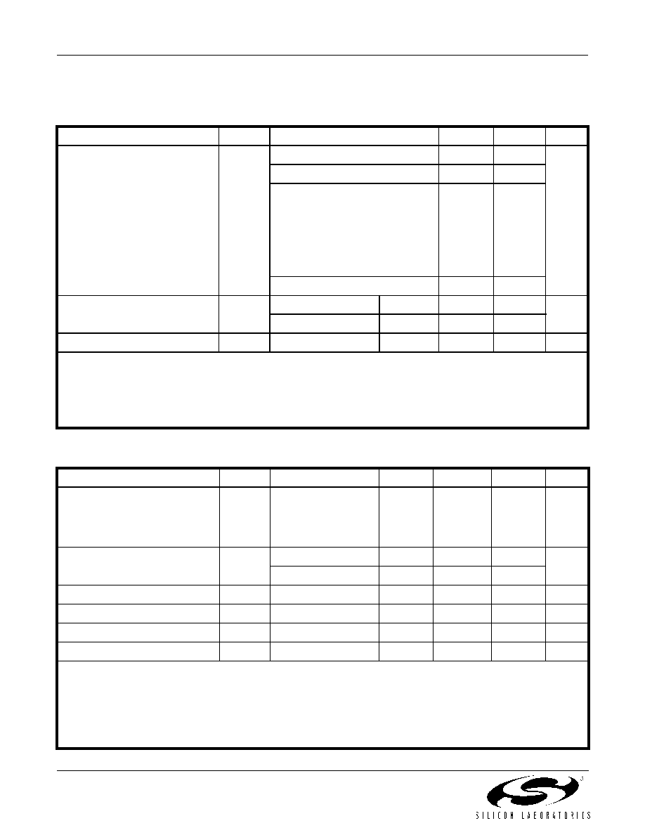
1. Electrical Specifications
Table 1. Recommended Operating Conditions
Parameter
Symbol
Test Condition
Min
Typ
Max
Units
Supply Voltage1
VDD
3.3 V option
2.97
3.3
3.63
V
2.5 V option
2.25
2.5
2.75
1.8 V option
1.71
1.8
1.89
Supply Current
IDD
Output enabled
LVPECL
CML
LVDS
CMOS
—
120
108
99
90
130
117
108
98
mA
TriState mode
—
60
70
Output Enable (OE)
and Frequency Select FS[1:0]2
VIH
0.75 x VDD
——
V
VIL
——
0.5
Operating Temperature Range3
TA
–40
—
85
C
Notes:
1. Selectable parameter specified by part number. See Section 3. "Ordering Information" on page 7 for further details.
2. OE and FS[1:0] pins include a 17 k
pullup resistor to VDD. Pulling OE to ground causes outputs to tristate.
3. If the device is powered up below –20 C and the ambient temperature rises by approximately 105 C during normal
operation, the device will perform a one-time recalibration. The output is squelched for approximately 2–3 ms during
this recalibration.
Table 2. VC Control Voltage Input
Parameter
Symbol
Test Condition
Min
Typ
Max
Units
Control Voltage Tuning Slope1,2,3
KV
10 to 90% of VDD
—45
90
135
180
—
ppm/V
Control Voltage Linearity4
LVC
BSL
–5
±1
+5
%
Incremental
–10
±5
+10
Modulation Bandwidth
BW
9.3
10.0
10.7
kHz
VC Input Impedance
ZVC
500
—
k
Nominal Control Voltage
VCNOM
@ fO
—3/8 x VDD
—V
Control Voltage Tuning Range
VC
0VDD
V
Notes:
1. Positive slope; selectable option by part number. See Section 3. "Ordering Information" on page 7.
2. For best jitter and phase noise performance, always choose the smallest KV that meets the application’s minimum APR
requirements. See “AN266: VCXO Tuning Slope (KV), Stability, and Absolute Pull Range (APR)” for more information.
3. KV variation is ±28% of typical values.
4. BSL determined from deviation from best straight line fit with VC ranging from 10 to 90% of VDD. Incremental slope
determined with VC ranging from 10 to 90% of VDD.
相關PDF資料 |
PDF描述 |
|---|---|
| 554AE000013BG | VCXO, CLOCK, 400 MHz, LVPECL OUTPUT |
| 550CF52M0000BG | VCXO, CLOCK, 52 MHz, CMOS OUTPUT |
| 552FC000139BGR | VCXO, CLOCK, 29.5 MHz, LVDS OUTPUT |
| 550AB595M000BGR | VCXO, CLOCK, 595 MHz, LVPECL OUTPUT |
| 550AE270M000BG | VCXO, CLOCK, 270 MHz, LVPECL OUTPUT |
相關代理商/技術參數(shù) |
參數(shù)描述 |
|---|---|
| 554AD000260DG | 制造商:Silicon Laboratories Inc 功能描述:OSCILLATOR - Trays |
| 554AD000260DGR | 制造商:Silicon Laboratories Inc 功能描述:OSCILLATOR - Tape and Reel |
| 554AD000290DG | 制造商:Silicon Laboratories Inc 功能描述:CNTRLD OSC 132.8125MHZ/155.52MHZ/156.25MHZ/166.63MHZ VCXO LV - Trays |
| 554AD000290DGR | 制造商:Silicon Laboratories Inc 功能描述:CNTRLD OSC 132.8125MHZ/155.52MHZ/156.25MHZ/166.63MHZ VCXO LV - Tape and Reel |
| 554AD000379DG | 功能描述:VCXO振蕩器 Quad VCXO 7mmx5mm 8 pin RoHS:否 制造商:Fox 封裝 / 箱體:5 mm x 3.2 mm 頻率:19.2 Mhz 頻率穩(wěn)定性:2.5 PPM 輸出格式: 封裝:Reel 電源電壓:3 V 端接類型:SMD/SMT 尺寸:3.2 mm W x 5 mm L x 1.5 mm H 最小工作溫度:- 20 C 最大工作溫度:+ 75 C |
發(fā)布緊急采購,3分鐘左右您將得到回復。