- 您現(xiàn)在的位置:買賣IC網(wǎng) > PDF目錄63241 > 545 SPECIALTY ANALOG CIRCUIT, DMA25 PDF資料下載
參數(shù)資料
| 型號(hào): | 545 |
| 元件分類: | 模擬信號(hào)調(diào)理 |
| 英文描述: | SPECIALTY ANALOG CIRCUIT, DMA25 |
| 文件頁數(shù): | 2/5頁 |
| 文件大?。?/td> | 513K |
| 代理商: | 545 |
A
2
CALEX
FaxFACTS:
324
1997
Models 545 and 546 Voltsensors
http://www.calex.com
2401 Stanwell Drive
Concord, CA 94520-4841
(510) 687-4411 Fax (510) 687-3333
The Amplifier Section
The input amplifier of the 545 and 546 is a true instrumentation
amplifier. This amplifier simply multiplies the difference
between the input pins by the gain. The gain is set by selecting
the gain pin required. The gain of the 545 is 10 to 1000 and
the 546 is 1 to 100. The pin selection, trip range and gain of
the two Voltsensors is shown on the following table.
The amplifier input voltage on both the 545 and 546 can be
as high as ±100 Volts without damage. The trip point range
is the main criteria for your Voltsensor selection and not the
maximum input voltage.
The Comparator Section
There are two comparators in the 545 and 546. They monitor
the output of the input amplifier for a signal too high and for
a signal too low. The actual trip point of each comparator is
set by the voltage on its associated potentiometer. The
relationship between the trip point voltage and the input is the
potentiometer voltage divided by the gain of the amplifier. If,
for example, the pot voltage was 6.5 Volts and the input
amplifier had a gain of ten, the trip point would be approximately
650 mV. Both the high and low comparators can be externally
programmed to latch and to provide a variable hysteresis.
The Output Section
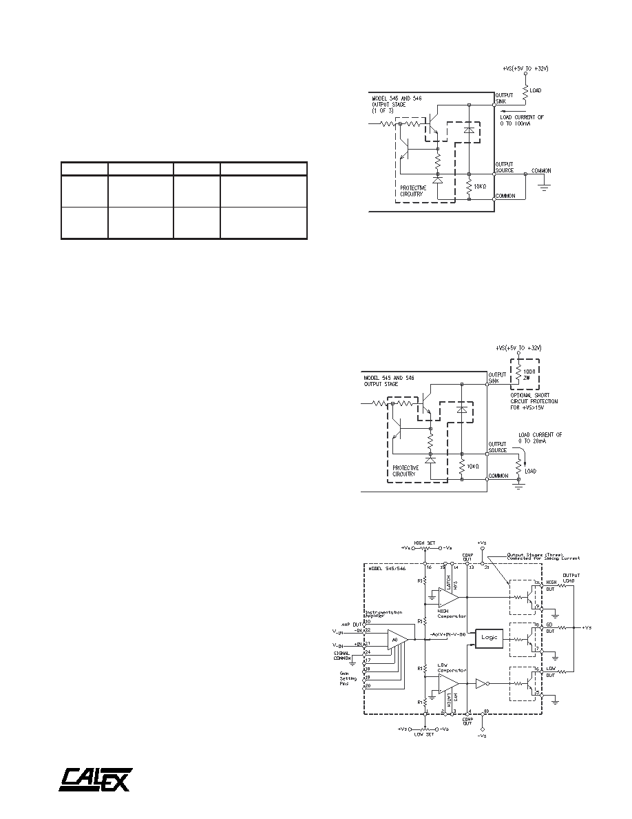
Current-Sinking Mode
Connections for current-sinking operation are shown in Figure
6. Each of the three outputs, Hl, GO and LO, are identical and
each is independent. When the base drive from the comparison
stages (or from the GO logic) swings positive, the output
transistor saturates and the load current flows through the
load and output transistor. The voltage across the collector-
to-emitter of the saturated transistor is very low and this logic
state is referred to as the “l(fā)ow state.” Output voltage in the low
state is approximately 0.1V plus IL x Rsat, where IL is the load
current and Rsat is the saturation impedance (typically 5
).
The saturation voltage at maximum load current is specified
to be less than 0.7V. When the base drive from the comparison
stages swings negative, the output transistor becomes cut-
off and the load current is switched off. The output voltage
then rises to the positive load voltage. Leakage from the cut-
off output transistor will be less than 1 A.
Power dissipation in the current-sinking mode is very low. In
the low state the output voltage is small although the current
is high. In the high state, the output voltage is high, but the
load current is small. For both conditions, the product of
output-voltage-times-loadcurrent is small and power
dissipation is minimal. For this reason, current-sinking is
generally preferred.
FIGURE 6.
Models 545 and 546, Connected for Current-Sinking Mode (One of
Three Outputs)
FIGURE 8.
Simplified Circuit Diagram for Models 545 and 546
FIGURE 7.
Models 545 and 546, Connected for Current-Sourcing Mode (One of
Three Outputs)
Current-Sourcing Mode
Any of the three outputs, Hl, GO, and LO, can be connected
as emitter-followers (see Figure 7). Each output is identical
and is independent of the other output stages. The output
voltages with all three connected as emitter followers are
shown in Figure 7. Each output can source up to +20mA and
each is short-circuit protected .
l
e
d
o
Me
g
n
a
R
p
i
r
Tn
i
a
Gm
a
r
g
o
r
P
n
i
P
5
4
5
V
m
0
1
-
0
V
m
0
1
-
0
V
1
-
0
1
0
1
0
1
0
2
-
9
1
n
i
p
r
e
p
m
u
J
0
2
-
8
1
n
i
p
r
e
p
m
u
J
.
d
’
q
e
R
r
e
p
m
u
J
o
N
6
4
5
V
m
0
1
-
0
V
1
-
0
V
0
1
-
0
1
0
1
0
2
-
9
1
n
i
p
r
e
p
m
u
J
0
2
-
8
1
n
i
p
r
e
p
m
u
J
.
d
’
q
e
R
r
e
p
m
u
J
o
N
相關(guān)PDF資料 |
PDF描述 |
|---|---|
| 54752001Z5V103Z | 1 FUNCTIONS, 250 V, 15 A, FEED THROUGH CAPACITOR |
| 54FCT521LB | COMPARATOR, QCC20 |
| 54FCT521DB | COMPARATOR, CDIP20 |
| 54FCT521CLB | COMPARATOR, QCC20 |
| 54FCT521CDB | COMPARATOR, CDIP20 |
相關(guān)代理商/技術(shù)參數(shù) |
參數(shù)描述 |
|---|---|
| 545 16 064 00 | 功能描述:電源變壓器 POWER TRANSFORMER RoHS:否 制造商:Triad Magnetics 功率額定值:12 VA 初級(jí)電壓額定值:115 V / 230 V 次級(jí)電壓額定值:12 V / 24 V 安裝風(fēng)格:SMD/SMT 一次繞組:Dual Primary Winding 二次繞組:Dual Secondary Winding 長度:2.5 in 寬度:2 in 高度:1.062 in |
| 545 23 225 00 | 制造商:Sumida Corporation 功能描述:POWER INDUCTOR UNSHIELDED |
| 545 23 320 00 | 制造商:Sumida Corporation 功能描述:- Tape and Reel |
| 545 24 027 00 | 制造商:Sumida Corporation 功能描述:POWER INDUCTOR UNSHIELDED |
| 545 BK078 | 功能描述:交流電源線 18AWG 3C UNSHLD 25PC PKG. BLACK RoHS:否 制造商:Schaffner 地區(qū):North American 插頭:NEMA 5-15P 插座:C13 Locking 功率額定值:2500 W 電流額定值:10 A 線規(guī) - 美國線規(guī)(AWG):18 電壓額定值:250 V 長度:6 ft 屏蔽: 外殼顏色:Black |
發(fā)布緊急采購,3分鐘左右您將得到回復(fù)。