- 您現(xiàn)在的位置:買賣IC網 > PDF目錄371605 > 522967B IC SMD PDF資料下載
參數(shù)資料
| 型號: | 522967B |
| 英文描述: | IC SMD |
| 中文描述: | 集成電路貼片 |
| 文件頁數(shù): | 7/12頁 |
| 文件大小: | 287K |
| 代理商: | 522967B |

7
LT1175
normally a good thing when the regulator is used by itself,
but it prevents the user from shutting down the regulator
when a second power source is connected to the LT1175
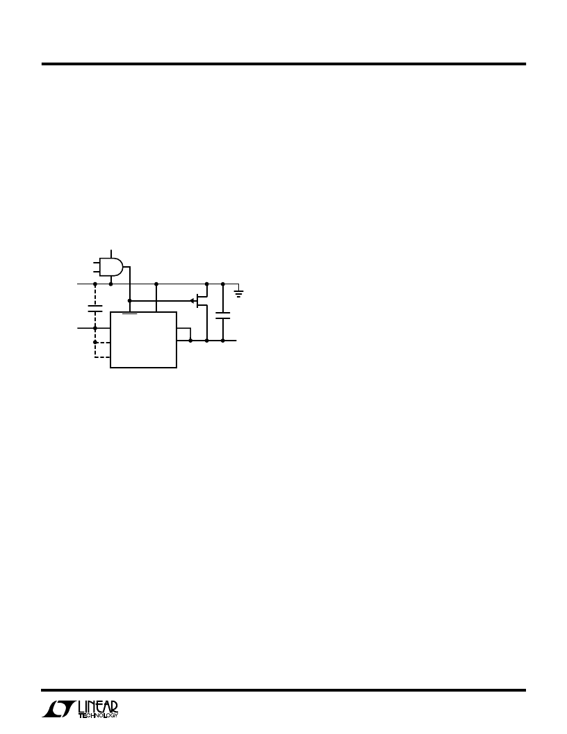
output. If active output pull-down is needed in shutdown,
it can be added externally with a depletion mode PFET as
shown in Figure 2. Note that the maximum pinch-off
voltage of the PFET must be less than the positive logic
high level to ensure that the device is completely off when
the regulator is active. The Motorola J177 device has
300
on resistance for zero gate source voltage.
APPLICATIO
S I
N
FOR
ATIO
U
W
U
yet allows the power transistor to approach its theoretical
saturation limit.
Output Capacitor
Several new regulator design techniques are used to make
the LT1175 extremely tolerant of output capacitor selec-
tion. Like most low dropout designs which use a collector
or drain of the power transistor to drive the output node,
the LT1175 uses the output capacitor as part of the overall
loop compensation. Older regulators generally required
the output capacitor to have a minimum value of 1
μ
F to
100
μ
F, a maximumESR (Effective Series Resistance) of
0.1
to 1
and a minimumESR in the range of 0.03
to
0.3
. These restrictions usually could be met only with
good quality solid tantalum capacitors. Aluminum capaci-
tors have problems with high ESR unless much higher
values of capacitance are used (physically large). The ESR
of ceramic or film capacitors was too low which made the
capacitance/ESR zero frequency too high to maintain
phase margin in the regulator. Even with optimum capaci-
tors, loop phase margin was very low in previous designs
when output current was low. These problems led to a new
design technique for the LT1175 error amplifier and inter-
nal frequency compensation as shown in Figure 3.
A conventional regulator loop consists of error amplifier
A1, driver transistor Q2 and power transistor Q1. Added to
this basic loop are secondary loops generated by Q3 and
C
F
. A DC negative feedback current fed into the error
amplifier through Q3 and R
N
causes overall loop current
gain to be very low at light load currents. This is not a
problem because very little gain is needed at light loads. In
addition to low gain, the parasitic pole frequency at Q2
base is extended by the DC feedback. The combination of
these two effects dramatically improves loop phase mar-
gin at light loads and makes the loop tolerant of large ESR
in the output capacitor. With heavy loads, loop phase and
gain are not nearly as troublesome and large negative
feedback could degrade regulation. The logarithmic behav-
ior of the base emitter voltage of Q1 reduces Q3 negative
feedback at heavy loads to prevent poor regulation.
In a conventional design, even with the nonlinear feed-
back, poor loop phase margin would occur at medium to
heavy loads if the ESR of the output capacitor fell below
+
C
OUT
≥
0.1
μ
F
–V
IN
Q1*
d
s
SHDN
GND
3V TO 5V
LT1175-5
SENSE
OUT
1175 F02
I
LIM4
I
LIM2
INPUT
* MOTOROLA J177
PINCH-OFF VOLTAGE MUST BE LESS THAN
POSITIVE LOGIC HIGH VOLTAGE
Minimum Dropout Voltage
Dropout voltage is the minimum voltage required between
input and output to maintain proper output regulation. For
older 3-terminal regulator designs, dropout voltage was
typically 1.5V to 3V. The LT1175 uses a saturating power
transistor design which gives much lower dropout volt-
age, typically 100mV at light loads and 450mV at full load.
Special precautions were taken to ensure that this tech-
nique does not cause quiescent supply current to be high
under light load conditions. When the regulator input
voltage is too low to maintain a regulated output, the pass
transistor is driven hard by the error amplifier as it tries to
maintain regulation. The current drawn by the driver
transistor could be tens of milliamperes even with little or
no load on the output. This indeed was the case for older
IC designs that did not actively limit driver current when
the power transistor saturated. The LT1175 uses a new
antisaturation technique that prevents high driver current,
Figure 2. Active Output Pull-Down During Shutdown
相關PDF資料 |
PDF描述 |
|---|---|
| 522968X | Dual/Triple Ultra-Low-Voltage SOT23 µP Supervisory Circuits |
| 522971X | IC |
| 522976X | IC |
| 522977R | Dual/Triple Ultra-Low-Voltage SOT23 µP Supervisory Circuits |
| 522978G | IC-SWITCHING REGULATOR |
相關代理商/技術參數(shù) |
參數(shù)描述 |
|---|---|
| 522968X | 制造商:未知廠家 制造商全稱:未知廠家 功能描述:IC |
| 522969R | 制造商:未知廠家 制造商全稱:未知廠家 功能描述:IC SMD |
| 522970A | 制造商:未知廠家 制造商全稱:未知廠家 功能描述:IC |
| 522-97-108-12-051-001 | 制造商:PREDIP 制造商全稱:Precid-Dip Durtal SA 功能描述:Pin grid array sockets / interconnect receptacle and pin / solder tail Receptacle with wire-wrap posts |
| 522971X | 制造商:未知廠家 制造商全稱:未知廠家 功能描述:IC |
發(fā)布緊急采購,3分鐘左右您將得到回復。