- 您現(xiàn)在的位置:買賣IC網(wǎng) > PDF目錄371605 > 522964H Dual/Triple Ultra-Low-Voltage SOT23 µP Supervisory Circuits PDF資料下載
參數(shù)資料
| 型號(hào): | 522964H |
| 英文描述: | Dual/Triple Ultra-Low-Voltage SOT23 µP Supervisory Circuits |
| 中文描述: | IC-SM-DC/DC轉(zhuǎn)爐 |
| 文件頁數(shù): | 5/12頁 |
| 文件大?。?/td> | 287K |
| 代理商: | 522964H |

5
LT1175
TYPICAL PERFOR
M
A
CE CHARACTERISTICS
U
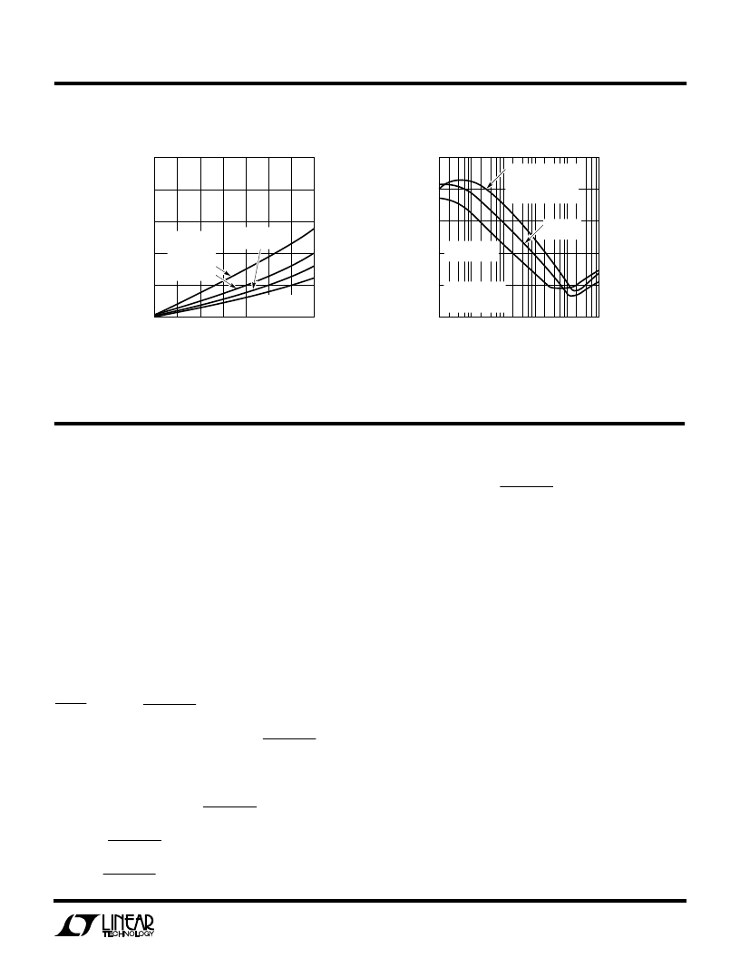
OUTPUT CURRENT (A)
0
G
20
16
12
8
4
0
0.2
0.4
0.3
0.5
1175 G10
0.1
0.6
0.7
POWER
TRANSISTOR
IN DROPOUT
T
J
= –55
°
C
T
J
= 25
°
C
V
IN
– V
OUT
≥
3V
T
J
= 25
°
V
IN
– V
=
2V
T
J
= 25
°
C
Ground Pin Current
FREQUENCY (Hz)
R
100
80
60
40
20
0
10
1k
10k
1M
100
100k
V
OUT
= 12V
(ADJUSTABLE)
I
OUT
= 100mA
V
IN
– V
OUT
= 2V
C
OUT
= 1
μ
F TANT
1175 G11
RIPPLE REJECTION IS RELATIVELY INDEPENDENT OF
INPUT VOLTAGE AND LOAD FOR CURRENTS BETWEEN
25mA AND 500mA. LARGER OUTPUT CAPACITORS DO
NOT IMPROVE REJECTION FOR FREQUENCIES BELOW
50kHz. AT VERY LIGHT LOADS, REJECTION WILL
IMPROVE WITH LARGER OUTPUT CAPACITORS
V
= 12V
(ADJUSTABLE)
WITH 0.1
μ
F ACROSS
DIVIDER RESISTOR
V
= 5V
(FIXED)
Ripple Rejection
current (see Typical Performance Characteristics). Maxi-
mum voltage on the Shutdown pin is 15V, –20V with
respect to the Ground pin and 35V, –5V with respect to the
negative Input pin.
I
LIM
Pins:
The two Current Limit pins are emitter sections
of the power transistor. When left open, they float several
hundred millivolts above the negative input voltage. When
shorted to the input voltage, they increase current limit by
a minimum of 200mA for I
LIM2
and 400mA for I
LIM4
. These
pins must be connected only to the input voltage, either
directly or through a resistor.
OUTPUT Pin:
The Output pin is the collector of the NPN
power transistor. It can be forced to the input voltage, to
ground or up to 2V positive with respect to ground without
damage or latchup (see Output Voltage Reversal in Appli-
cations Information section). The LT1175 has foldback
current limit, so maximum current at the Output pin is a
function of input-to-output voltage. See Typical Perfor-
mance Characteristics.
GND Pin:
The Ground pin has a quiescent current of 45
μ
A
at zero load current, increasing by approximately 10
μ
A per
mA of output current. At 500mA output current, Ground pin
current is about 5mA. Current flows into the Ground pin.
SENSE Pin:
The Sense pin is used in the adjustable version
to allow custom selection of output voltage, with an
external divider set to generate 3.8V at the Sense pin. Input
bias current is typically 75nA flowing out of the pin.
Maximum forced voltage on the Sense pin is 2V and –10V
with respect to Ground pin.
The fixed 5V version utilizes the Sense pin to give true
Kelvin connections to the load or to drive an external pass
transistor for higher output currents. Bias current out of
the 5V Sense pin is approximately 12
μ
A. Separating the
Sense and Output pins also allows for a new loop compen-
sation technique described in the Applications Informa-
tion section.
SHDN Pin:
The Shutdown pin is specially configured to
allow it to be driven from either positive voltage logic or
with negative only logic. Forcing the Shutdown pin 2V
either above or below the Ground pin will turn the regulator
on. This makes it simple to connect directly to positive
logic signals for active low shutdown. If no positive
voltages are available, the Shutdown pin can be driven
below the Ground pin to turn the regulator on. When left
open, the Shutdown pin will default ow to a regulator “on”
condition For all voltages below absolute maximum rat-
ings, the Shutdown pin draws only a few microamperes of
PI
FU
CTIO
N
S
U
U
相關(guān)PDF資料 |
PDF描述 |
|---|---|
| 522965F | IC-SWITCHING REGULATOR |
| 522966D | Dual/Triple Ultra-Low-Voltage SOT23 µP Supervisory Circuits |
| 522967B | IC SMD |
| 522968X | Dual/Triple Ultra-Low-Voltage SOT23 µP Supervisory Circuits |
| 522971X | IC |
相關(guān)代理商/技術(shù)參數(shù) |
參數(shù)描述 |
|---|---|
| 522965F | 制造商:未知廠家 制造商全稱:未知廠家 功能描述:IC-SWITCHING REGULATOR |
| 522966D | 制造商:未知廠家 制造商全稱:未知廠家 功能描述:IC |
| 522967B | 制造商:未知廠家 制造商全稱:未知廠家 功能描述:IC SMD |
| 522968X | 制造商:未知廠家 制造商全稱:未知廠家 功能描述:IC |
| 522969R | 制造商:未知廠家 制造商全稱:未知廠家 功能描述:IC SMD |
發(fā)布緊急采購,3分鐘左右您將得到回復(fù)。