- 您現(xiàn)在的位置:買賣IC網(wǎng) > PDF目錄371561 > 508591B IC SMD PDF資料下載
參數(shù)資料
| 型號(hào): | 508591B |
| 英文描述: | IC SMD |
| 中文描述: | 集成電路貼片 |
| 文件頁(yè)數(shù): | 9/16頁(yè) |
| 文件大?。?/td> | 278K |
| 代理商: | 508591B |
第1頁(yè)第2頁(yè)第3頁(yè)第4頁(yè)第5頁(yè)第6頁(yè)第7頁(yè)第8頁(yè)當(dāng)前第9頁(yè)第10頁(yè)第11頁(yè)第12頁(yè)第13頁(yè)第14頁(yè)第15頁(yè)第16頁(yè)

9
LT1083/LT1084/LT1085
APPLICATIO
S I
N
FOR
ATIO
U
The problem occurs with a heavy output load when the
input voltage is high and the output voltage is low, such as
immediately after removal of a short. The load line for such
a load may intersect the output current curve at two points.
If this happens, there are two stable output operating
points for the regulator. With this double intersection, the
power supply may need to be cycled down to zero and
brought up again to make the output recover.
W
U
Ripple Rejection
The typical curves for ripple rejection reflect values for a
bypassed adjustment pin. This curve will be true for all
values of output voltage. For proper bypassing and ripple
rejection approaching the values shown, the impedance of
the adjust pin capacitor at the ripple frequency should be
less than the value of R1, (normally 100
to 120
). The
size of the required adjust pin capacitor is a function of the
input ripple frequency. At 120Hz the adjust pin capacitor
should be 25
μ
F if R1 = 100
. At 10kHz only 0.22
μ
F is
needed.
For circuits without an adjust pin bypass capacitor, the
ripple rejection will be a function of output voltage. The
output ripple will increase directly as a ratio of the output
voltage to the reference voltage (V
OUT
/V
REF
). For example,
with the output voltage equal to 5V and no adjust pin
capacitor, the output ripple will be higher by the ratio of 5V/
1.25V or four times larger. Ripple rejection will be de-
graded by 12dB from the value shown on the typical curve.
Output Voltage
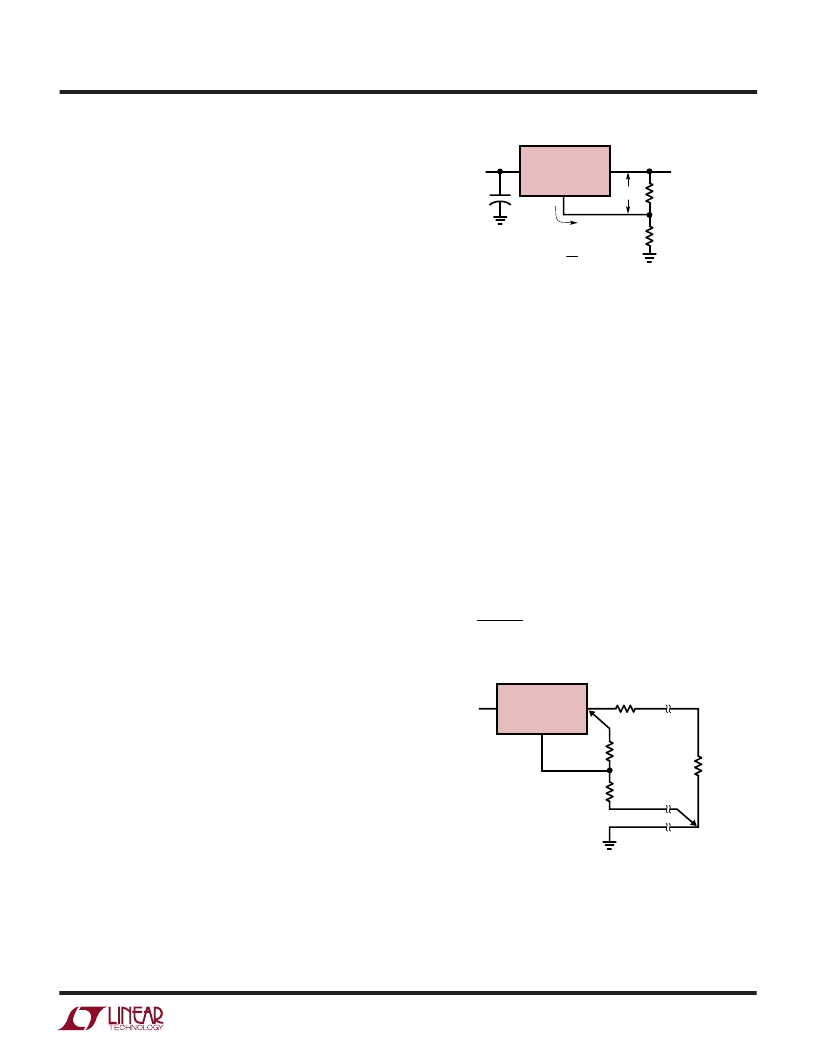
The LT1083 develops a 1.25V reference voltage between
the output and the adjust terminal (see Figure 1). By
placing a resistor R1 between these two terminals, a
constant current is caused to flow through R1 and down
through R2 to set the overall output voltage. Normally this
current is the specified minimum load current of 10mA.
Because I
ADJ
is very small and constant when compared
with the current through R1, it represents a small error and
can usually be ignored.
Figure 1. Basic Adjustable Regulator
R1
R2
IN
OUT
I
ADJ
50
A
ADJ
V
OUT
LT1083
V
IN
1083/4/5 ADJ F01
V
REF
V
OUT
= V
REF
1 + R1
ADJ
R2
(
)
Load Regulation
Because the LT1083 is a three-terminal device, it is not
possible to provide true remote load sensing. Load regu-
lation will be limited by the resistance of the wire connect-
ing the regulator to the load. The data sheet specification
for load regulation is measured at the bottom of the
package. Negative side sensing is a true Kelvin connec-
tion, with the bottom of the output divider returned to the
negative side of the load. Although it may not be immedi-
ately obvious, best load regulation is obtained when the
top of the resistor divider R1 is connected directlyto the
case not to the load This is illustrated in Figure 2. If R1
were connected to the load, the effective resistance be-
tween the regulator and the load would be:
R
R
R
R
R
Parasitic Line
P
P
×
+
=
2
1
1
,
Resistance
Figure 2. Connections for Best Load Regulation
LT1083
OUT
IN
V
IN
ADJ
R
PARASITIC
LINE RESISTANCE
R1*
*CONNECT R1 TO CASE
CONNECT R2 TO LOAD
1083/4/5 ADJ F02
R
L
R2*
相關(guān)PDF資料 |
PDF描述 |
|---|---|
| 522970A | Dual/Triple Ultra-Low-Voltage SOT23 µP Supervisory Circuits |
| 505PWSM | ROLLENAUFWICKLER MINI NADELDRUCKER |
| 50620MLLNF | Dual/Triple Ultra-Low-Voltage SOT23 µP Supervisory Circuits |
| 50620 | GLAND EMC M20 |
| 5062 | Dual/Triple Ultra-Low-Voltage SOT23 µP Supervisory Circuits |
相關(guān)代理商/技術(shù)參數(shù) |
參數(shù)描述 |
|---|---|
| 508593R | 制造商:未知廠家 制造商全稱:未知廠家 功能描述:IC |
| 508595E | 制造商:未知廠家 制造商全稱:未知廠家 功能描述:IC |
| 508596C | 制造商:未知廠家 制造商全稱:未知廠家 功能描述:IC |
| 508597112 | 制造商:MOLEX 制造商全稱:Molex Electronics Ltd. 功能描述:Ring Tongue Terminal for 4 AWG, Closed Uninsulated Brazed Barrel, Stud Size 10(M5), Oxygen-Free Copper, Length 33.40mm (1.315"), Clearance 15.50mm (.610") |
| 50859-7112 | 功能描述:端子 R22-S5 R22-S5 RoHS:否 制造商:AVX 產(chǎn)品:Junction Box - Wire to Wire 系列:9826 線規(guī):26-18 接線柱/接頭大小: 絕緣: 顏色:Red 型式:Female 觸點(diǎn)電鍍:Tin over Nickel 觸點(diǎn)材料:Beryllium Copper, Phosphor Bronze 端接類型:Crimp |
發(fā)布緊急采購(gòu),3分鐘左右您將得到回復(fù)。