- 您現(xiàn)在的位置:買賣IC網(wǎng) > PDF目錄30629 > 4127 (Texas Instruments, Inc.) Logarithmic Amplifier(對(duì)數(shù)放大器) PDF資料下載
參數(shù)資料
| 型號(hào): | 4127 |
| 廠商: | Texas Instruments, Inc. |
| 元件分類: | 對(duì)數(shù)放大器 |
| 英文描述: | Logarithmic Amplifier(對(duì)數(shù)放大器) |
| 中文描述: | 對(duì)數(shù)放大器(對(duì)數(shù)放大器) |
| 文件頁數(shù): | 4/8頁 |
| 文件大小: | 107K |
| 代理商: | 4127 |
4
4127
From the semiconductor junction characteristics, the base-
to-emitter voltage will be:
V
BE ≈
n
,
where: I
C = Collector current
I
L = Reverse saturation current
q, m, K = Constants
T = Absolute temperature
So E
1 = –
n
and E
2 – E1 =
n
If the transistors Q
1 and Q2 are at the same temperature and
have matched characteristics, then:
E
2 =
n
–
n
E
2 =
n
The output op amp, A
2, provides a voltage gain of approxi-
mately (R
T + R2)/RT, and the value of (mKT)/q is about
26mV at room temperature. Since resistor R
T varies with
temperature to compensate for gain drift, the output voltage,
E
O, expressed as a log will be:
mic functions, including the log ratio of two signals, the
logarithm of an input signal, or the antilog of an input signal.
The unique FET-input current-inverting element removes
the polarity limitations present in most conventional log
amplifiers.
Utilizing the inherent exponential characteristics of transis-
tor functions, the 4127 calculates accurate log functions for
input currents from 1nA to 1mA, or input voltages from
1mV to 10V. Carefully matched monolithic quad transistors
and temperature sensitive gain elements are used to produce
a log amplifier with excellent temperature characteristics.
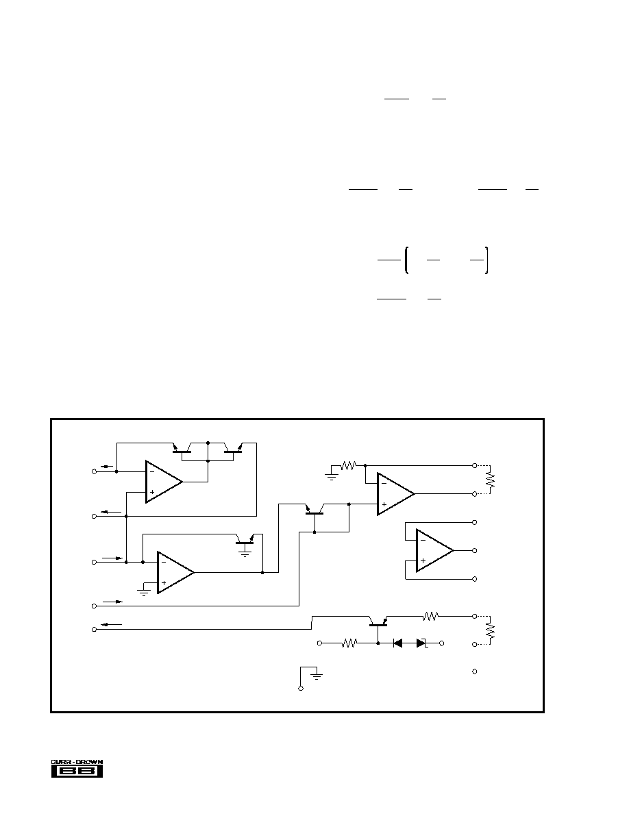
A functional diagram of the 4127 circuit is shown in
Figure 1. In addition to the basic log amplifier, the 4127
contains a separate internal current source, a current
inverter, and an uncommitted operational amplifier. The
current inverter accurately converts negative input current to
a positive current of equal magnitude.
The 4127 is capable of accurately logging input current over
a 120dB range, but to use this full range, good shielding
practice must be followed. A current source input is, by
definition, a high impedance source and is therefore subject
to electrostatic pickup.
The input op amps, A
1 and A3, have FET input stages for low
noise and very-low input bias current. The op amp, A
1, will
make the collector current of Q
1 equal to the signal input
current I
S,
and the collector current of Q
2
will be the
reference input current I
R.
mKT
q
I
L
I
C
I
L
I
R
I
L
I
S
I
R
I
S
FIGURE 1. Functional Diagram.
mKT
1
q
I
L1
I
S
mKT
2
q
I
L2
I
R
–mKT
q
mKT
q
l
+15VDC
–15VDC
19
18
A
2
A
4
10
11
9
23
22
14
–15VDC
+15VDC
I
R
1
I
REF
Op Amp
+Input
Op Amp
Output
Op Amp
–Input
Log Output
Gain
Adjust
5k
21
Common
A
3
A
1
≈520 Thermistor
Q
2
E
2
R
T
E
O
Q
1
E
1
7
4
2
+I
INPUT
5
1
Current
Inverter
Input
Current
Inverter
Output
I
REF
Input
I
REF
Output
I
R
I
S
I
S
I
R
I
S
R
2
Gain
相關(guān)PDF資料 |
PDF描述 |
|---|---|
| 41680 | Toroidal Surface Mount Inductors |
| 416R8 | Toroidal Surface Mount Inductors |
| 41100 | Toroidal Surface Mount Inductors |
| 41101 | Toroidal Surface Mount Inductors |
| 41150 | Toroidal Surface Mount Inductors |
相關(guān)代理商/技術(shù)參數(shù) |
參數(shù)描述 |
|---|---|
| 412-7 | 功能描述:旋鈕開關(guān) 7 TAPS 50A/300VAC 20VDC RoHS:否 制造商:C&K Components 位置數(shù)量:5 卡片組數(shù)量: 每卡片組極數(shù):2 電流額定值:250 mA 電壓額定值:125 V 指數(shù)角: 觸點(diǎn)類型: 觸點(diǎn)形式:DPST 端接類型:Solder 安裝類型:Panel 觸點(diǎn)電鍍:Silver |
| 41270.07 | 制造商:Vynckier Enclosure Systems Inc 功能描述:APO CARRY HANDLE |
| 412700000 | 功能描述:開關(guān)配件 STACKING SCREW 3XXX .950 RoHS:否 制造商:C&K Components 類型:Cap 用于:Pushbutton Switches 設(shè)計(jì)目的: |
| 4127010 | 制造商:Rittal 功能描述:DOOR SWITCH UL |
| 412701000 | 功能描述:開關(guān)配件 SCRW 3-4 FRNT 3 REAR RoHS:否 制造商:C&K Components 類型:Cap 用于:Pushbutton Switches 設(shè)計(jì)目的: |
發(fā)布緊急采購,3分鐘左右您將得到回復(fù)。