- 您現(xiàn)在的位置:買(mǎi)賣(mài)IC網(wǎng) > PDF目錄358638 > 3D7424D-2 (DATA DELAY DEVICES INC) MONOLITHIC QUAD 4-BIT PROGRAMMABLE DELAY LINE PDF資料下載
參數(shù)資料
| 型號(hào): | 3D7424D-2 |
| 廠商: | DATA DELAY DEVICES INC |
| 元件分類(lèi): | 通用總線功能 |
| 英文描述: | MONOLITHIC QUAD 4-BIT PROGRAMMABLE DELAY LINE |
| 中文描述: | ACTIVE DELAY LINE, TRUE OUTPUT, PDSO14 |
| 封裝: | ROHS COMPLIANT, SOIC-14 |
| 文件頁(yè)數(shù): | 1/6頁(yè) |
| 文件大?。?/td> | 176K |
| 代理商: | 3D7424D-2 |
3D7424
MONOLITHIC QUAD 4-BIT
PROGRAMMABLE DELAY LINE
(SERIES 3D7424)
FEATURES
Four indep’t programmable lines on a single chip
All-silicon CMOS technology
Low quiescent current (5mA typical)
Leading- and trailing-edge accuracy
Vapor phase, IR and wave solderable
Increment range:
0.75ns through 400ns
Delay tolerance:
3% or 2ns (see Table 1)
Line-to-line matching:
1% or 1ns typical
Temperature stability:
±
1.5% typical (-40C to 85C)
Vdd stability:
±
0.5% typical (4.75V to 5.25V)
Minimum input pulse width:
10% of total delay
FUNCTIONAL DESCRIPTION
The 3D7424 device is a small, versatile, quad 4-bit programmable
monolithic delay line. Delay values, programmed via the serial interface,
can be independently varied over 15 equal steps. The step size (in ns) is
determined by the device dash number. Each input is reproduced at the
corresponding output without inversion, shifted in time as per user
selection. For each line, the delay time is given by:
TD
n
= T0 + A
n
* TI
where T0 is the inherent delay, A
n
is the delay address of the n-th line
and TI is the delay increment (dash number). The desired addresses are
shifted into the device via the SC and SI inputs, and the addresses are latched using the AL input. The
serial interface can also be used to enable/disable each delay line. The 3D7424 operates at 5 volts and
has a typical T0 of 6ns. The 3D7424 is TTL/CMOS-compatible, capable of sourcing or sinking 4mA loads,
and features both rising- and falling-edge accuracy. The device is offered in a standard 14-pin auto-
insertable DIP and a space saving surface mount 14-pin SOIC.
TABLE 1: PART NUMBER SPECIFICATIONS
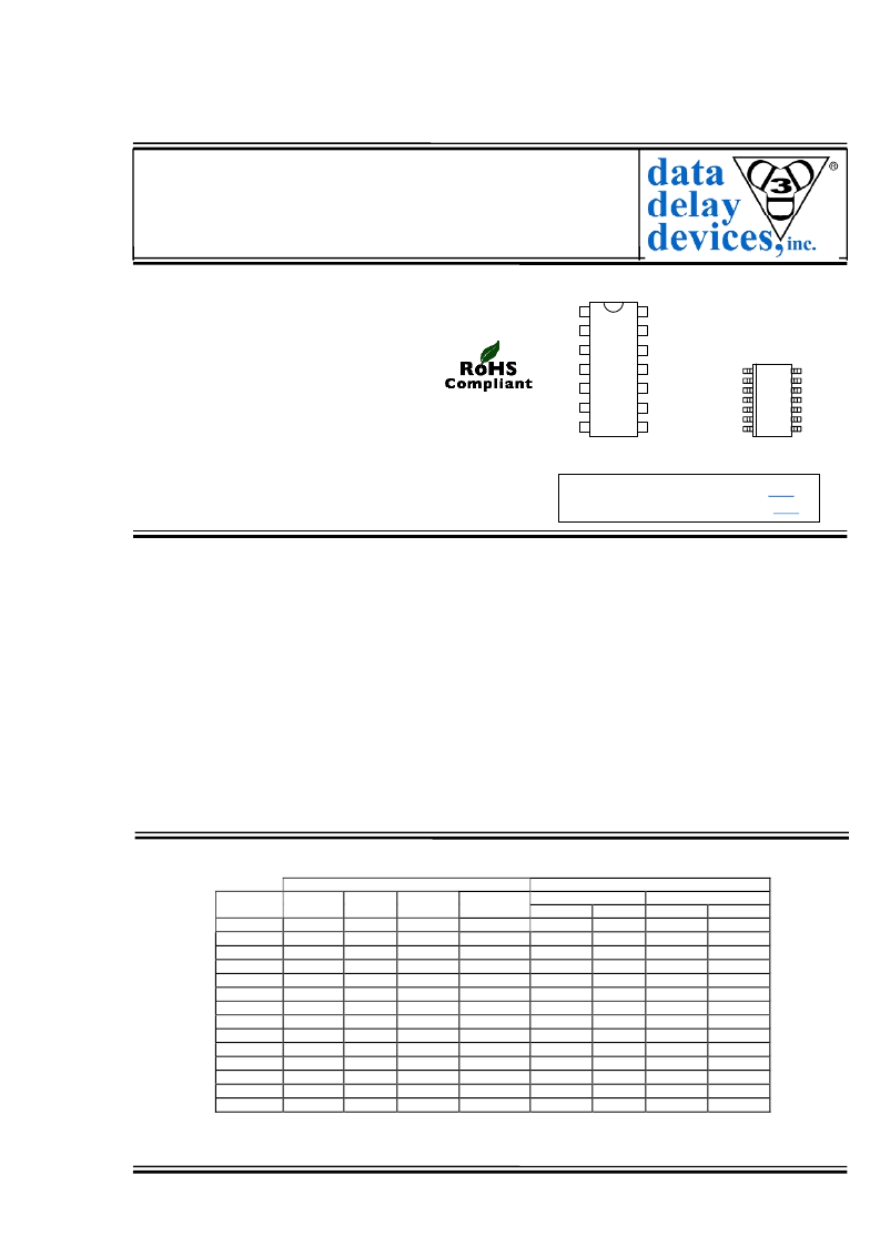
PACKAGES
14
13
12
11
10
9
8
1
2
3
4
5
6
7
I1
SC
I2
I3
I4
SI
GND
VDD
AL
O1
SO
O2
O3
O4
DIP-14
3D7424-xx
1
2
3
4
5
6
7
14
13
12
11
10
9
8
I1
SC
I2
I3
I4
SI
GND
VDD
AL
O1
SO
O2
O3
O4
SOIC-14
3D7424D-xx
PIN DESCRIPTIONS
I1-I4
Signal Inputs
O1-O4 Signal Outputs
AL
Address Latch In
SC
Serial Clock In
SI
Serial Data In
SO
Serial Data Out
VDD
5.0V
GND
Ground
For mechanical dimensions, click
here
.
For package marking details, click
here
.
DELAYS & TOLERANCES (NS)
Inherent
Delay
.75
±
0.19
6.0
±
2.0
1.0
±
0.25
6.0
±
2.0
1.5
±
0.38
6.0
±
2.0
2.0
±
0.50
6.0
±
2.0
4.0
±
1.00
6.0
±
2.0
5.0
±
1.25
6.0
±
2.0
10
±
2.50
6.0
±
2.0
15
±
3.75
6.0
±
2.0
20
±
5.00
6.0
±
2.0
40
±
10.0
6.0
±
2.0
50
±
10.0
6.0
±
2.0
100
±
12.5
6.0
±
2.0
200
±
20.0
6.0
±
2.0
400
±
40.0
6.0
±
2.0
NOTE: Any increment between 0.75ns and 400ns not shown is also available as standard
See page 4 for details regarding input restrictions
INPUT RESTRICTIONS
Max Frequency
Recom’d
Absolute
19 MHz
166 MHz
16 MHz
166 MHz
12 MHz
111 MHz
9.2 MHz
83 MHz
5.0 MHz
83 MHz
4.1 MHz
66 MHz
2.1 MHz
33 MHz
1.4 MHz
22 MHz
1.0 MHz
16 MHz
550 KHz
8.3 MHz
440 KHz
6.6 MHz
220 KHz
3.3 MHz
110 KHz
1.6 MHz
55 KHz
833 KHz
Min Pulse Width
Recom’d
26 ns
32 ns
43 ns
54 ns
99 ns
122 ns
234 ns
347 ns
459 ns
909 ns
1.2 us
2.3 us
4.5 us
9.0 us
Part
Number
3D7424-.75
3D7424-1
3D7424-1.5
3D7424-2
3D7424-4
3D7424-5
3D7424-10
3D7424-15
3D7424-20
3D7424-40
3D7424-50
3D7424-100
3D7424-200
3D7424-400
Delay
Step
Total
Delay
17.25
±
2.0 3% or 0.50ns
21.0
±
2.0 3% or 0.50ns
28.5
±
2.0 3% or 0.50ns
36.0
±
2.0 3% or 0.75ns
66.0
±
2.0 3% or 0.75ns
81.0
±
2.5 3% or 0.75ns
156
±
5.0 3% or 1.25ns
231
±
7.5 3% or 1.88ns
306
±
10 3% or 2.50ns
606
±
20 3% or 5.00ns
756
±
25 3% or 6.25ns
1506
±
50 3% or 12.5ns
3006
±
100 3% or 25.0ns
6006
±
200 3% or 50.0ns
Relative
Tolerance
Absolute
3.0 ns
3.0 ns
4.5 ns
6.0 ns
6.0 ns
7.5 ns
15.0 ns
22.5 ns
30.0 ns
60.0 ns
75.0 ns
150 ns
300 ns
600 ns
2006 Data Delay Devices
Doc #06019
6/5/2006
DATA DELAY DEVICES, INC.
3 Mt. Prospect Ave. Clifton, NJ 07013
1
相關(guān)PDF資料 |
PDF描述 |
|---|---|
| 3D7428-10 | MONOLITHIC 8-BIT PROGRAMMABLE DELAY LINE |
| 3D7428-15 | MONOLITHIC 8-BIT PROGRAMMABLE DELAY LINE |
| 3D7428-2 | MONOLITHIC 8-BIT PROGRAMMABLE DELAY LINE |
| 3D7428-2.5 | MONOLITHIC 8-BIT PROGRAMMABLE DELAY LINE |
| 3D7428-20 | MONOLITHIC 8-BIT PROGRAMMABLE DELAY LINE |
相關(guān)代理商/技術(shù)參數(shù) |
參數(shù)描述 |
|---|---|
| 3D7424D-20 | 制造商:DATADELAY 制造商全稱(chēng):Data Delay Devices, Inc. 功能描述:MONOLITHIC QUAD 4-BIT PROGRAMMABLE DELAY LINE |
| 3D7424D-200 | 制造商:DATADELAY 制造商全稱(chēng):Data Delay Devices, Inc. 功能描述:MONOLITHIC QUAD 4-BIT PROGRAMMABLE DELAY LINE |
| 3D7424D-4 | 制造商:DATADELAY 制造商全稱(chēng):Data Delay Devices, Inc. 功能描述:MONOLITHIC QUAD 4-BIT PROGRAMMABLE DELAY LINE |
| 3D7424D-40 | 制造商:DATADELAY 制造商全稱(chēng):Data Delay Devices, Inc. 功能描述:MONOLITHIC QUAD 4-BIT PROGRAMMABLE DELAY LINE |
| 3D7424D-400 | 制造商:DATADELAY 制造商全稱(chēng):Data Delay Devices, Inc. 功能描述:MONOLITHIC QUAD 4-BIT PROGRAMMABLE DELAY LINE |
發(fā)布緊急采購(gòu),3分鐘左右您將得到回復(fù)。