- 您現(xiàn)在的位置:買賣IC網(wǎng) > PDF目錄358628 > 34063A (Electronic Theatre Controls, Inc.) DC-TO-DC CONVERTER CONTROL CIRCUITS PDF資料下載
參數(shù)資料
| 型號(hào): | 34063A |
| 廠商: | Electronic Theatre Controls, Inc. |
| 英文描述: | DC-TO-DC CONVERTER CONTROL CIRCUITS |
| 中文描述: | 的DC - DC轉(zhuǎn)換器控制電路 |
| 文件頁(yè)數(shù): | 2/2頁(yè) |
| 文件大小: | 115K |
| 代理商: | 34063A |
ORDERING INFORMATION
Device
Temperature
Range
34063AD 0° to +70°C
34063AP1
ELECTRICAL CHARACTERICISTICS
(V
CC
= 5.0 V, T
A
= 0 to +70
C unless otherwise specified.)
Package
SO-8
Plastic DIP
Characteristics
Symbol
Min
Typ
Max
Unit
OSCILLATOR
Frequency (V
Pin 5
= 0 V, C
T
= 1.0 nF, T
A
= 25°C)
Charge Current (V
CC
= 5.0 V to 40 V, T
A
= 25°C)
Discharge Current (
V
CC
= 5.0 V to 40 V, T
A
= 25°C)
Discharge to Charge Current Ratio (Pin7 to Vcc, T
A
=25°C)
I
dischg
/I
chg
Current Limit Sense Voltage (Ichg = Idischg, T
A
= 25°C)
f
osc
I
chg
I
dischg
24
24
140
5.2
33
33
200
6.2
300
42
42
260
7.5
350
kHz
μ
A
μ
A
—
mV
V
lpk
(sense) 250
OUTPUT SWITCH (Note 3)
Saturation Voltage, Darlington Connection (I
SW
= 1.0 A,
Pins 1, 8 connected)
Saturation Voltage (I
SW
= 1.0 A, R
Pin 8
= 82
to V
CC
.
Forced
β
= 20)
DC Current Gain (I
SW
= 1.0 A, V
CE
=
5.0 V, T
A
= 25°C) h
FE
Collector Off-State Current (V
CE
= 40V)
V
CE
(sat)
—
1.0
1.3
V
V
CE
(sat)
—
0.45
0.7
V
50
—
120
0.01
—
100
—
μ
A
I
C
(off)
COMPARATOR
Threshold Voltage (T
A
= 25°C)
(T
A
= T
LOW
to T
HIGH
)
Vth
1.225
1.21
1.2375
—
1.25
—
1.25
1.4
-40
1.275
1.29
1.2625 V
V
Threshold Voltage (T
A
= 25°C) **
Vth
Threshold Voltage Line Regulation (V
CC
= 3.0 V to 40 V)
Input Bias Current (Vin=0V)
V
REG line
I
IB
5.0
-400
mV
nA
TOTAL DEVICE
Supply Current (V
CC
= 5 0 V to 40 V, C
T
= 1 0 nF, V
pin7
=
V
CC
. V
Pin5
> Vth, Pin 2 = Gnd, Remaining pins open)
NOTES:
1. Maximum package power dissipation limits must be observed.
2.
Low duty cycle pulse techniques are used during test to maintain Junction temperature as close to ambient
temperature as possible
3.
If the output switch is driven into hard saturation (non Darlington configuration) at low switch currents (< 300 mA) and
high driver
currents (>30 mA), it may take up to 2.0
μ
s to come out of saturation This condition will shorten the off' time
at frequencies > 30 kHz, and is magnified at high temperatures This condition does not occur with a Darlington configuration,
since the output switch cannot
saturate If a non Darlington configuration is used, the following output drive condition is
recommended
Forced
β
of output switch = I
C
, output/(Ic, driver -7.0 mA*) > 10
*The 100
.
resistor in the emitter of the driver device requires about 7.0 mA before the output switch conducts
**
Possible version for shipment
I
CC
2.5
4.0
mA
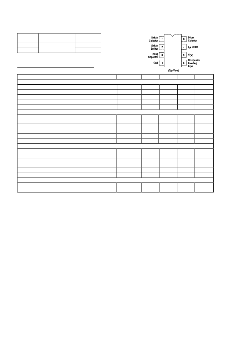
Pin connection
相關(guān)PDF資料 |
PDF描述 |
|---|---|
| 34063AD | DC-TO-DC CONVERTER CONTROL CIRCUITS |
| 34063AP1 | DC-TO-DC CONVERTER CONTROL CIRCUITS |
| 34063CM | 0.8A STEP-DOWN/STEP-UP/INVERTING DC-DC CONVERTER |
| 34280M1 | SINGLE-CHIP 4-BIT CMOS MICROCOMPUTER |
| 3429-5602UN | Ultra-Low-Power Voltage Detectors and µP Supervisory Circuits |
相關(guān)代理商/技術(shù)參數(shù) |
參數(shù)描述 |
|---|---|
| 34063AD | 制造商:未知廠家 制造商全稱:未知廠家 功能描述:DC-TO-DC CONVERTER CONTROL CIRCUITS |
| 34063AM | 制造商:BCDSEMI 制造商全稱:BCD Semiconductor Manufacturing Limited 功能描述:1.5A STEP-DOWN/STEP-UP/INVERTING DC-DC CONVERTER |
| 34063AM-E1 | 制造商:BCDSEMI 制造商全稱:BCD Semiconductor Manufacturing Limited 功能描述:1.5A STEP-DOWN/STEP-UP/INVERTING DC-DC CONVERTER |
| 34063AN | 制造商:IKSEMICON 制造商全稱:IK Semicon Co., Ltd 功能描述:DC-TO-DC CONVERTER CONTROL CIRCUITS |
| 34063AP1 | 制造商:未知廠家 制造商全稱:未知廠家 功能描述:DC-TO-DC CONVERTER CONTROL CIRCUITS |
發(fā)布緊急采購(gòu),3分鐘左右您將得到回復(fù)。