- 您現(xiàn)在的位置:買賣IC網(wǎng) > PDF目錄33501 > 2SK3576 4000 mA, 20 V, N-CHANNEL, Si, SMALL SIGNAL, MOSFET PDF資料下載
參數(shù)資料
| 型號: | 2SK3576 |
| 元件分類: | 小信號晶體管 |
| 英文描述: | 4000 mA, 20 V, N-CHANNEL, Si, SMALL SIGNAL, MOSFET |
| 封裝: | PLASTIC, SC-96, 3 PIN |
| 文件頁數(shù): | 1/7頁 |
| 文件大小: | 66K |
| 代理商: | 2SK3576 |
The information in this document is subject to change without notice. Before using this document, please
confirm that this is the latest version.
Not all devices/types available in every country. Please check with local NEC representative for
availability and additional information.
2001
MOS FIELD EFFECT TRANSISTOR
2SK3576
N-CHANNEL MOS FIELD EFFECT TRANSISTOR
FOR SWITCHING
DATA SHEET
Document No.
D15939EJ1V0DS00 (1st edition)
Date Published
May 2002 NS CP(K)
Printed in Japan
DESCRIPTION
The 2SK3576 is a switching device which can be driven
directly by a 2.5 V power source.
The device features a low on-state resistance and excellent
switching characteristics, and is suitable for applications such
as power switch of portable machine and so on.
FEATURES
2.5V drive available
Low on-state resistance
RDS(on)1 = 50 m
MAX. (VGS = 4.5 V, ID = 2.0 A)
RDS(on)2 = 53 m
MAX. (VGS = 4.0 V, ID = 2.0 A)
RDS(on)3 = 75 m
MAX. (VGS = 2.5 V, ID = 2.0 A)
ORDERING INFORMATION
PART NUMBER
PACKAGE
2SK3576
SC-96 (Mini Mold Thin Type)
Marking: XK
ABSOLUTE MAXIMUM RATINGS (TA = 25°C)
Drain to Source Voltage (VGS = 0 V)
VDSS
20
V
Gate to Source Voltage (VDS = 0 V)
VGSS
±12
V
Drain Current (DC) (TA = 25°C)
ID(DC)
±4.0
A
Drain Current (pulse)
Note1
ID(pulse)
±16
A
Total Power Dissipation (TA = 25°C)
PT1
0.2
W
Total Power Dissipation (TA = 25°C)
Note2
PT2
1.25
W
Channel Temperature
Tch
150
°C
Storage Temperature
Tstg
–55 to +150
°C
Notes 1. PW
≤ 10
s, Duty Cycle ≤ 1%
2. Mounted on FR-4 board, t
≤ 5 sec.
Remark The diode connected between the gate and source of the transistor serves as a protector against ESD. When
this device actually used, an additional protection circuit is externally required if a voltage exceeding the rated
voltage may be applied to this device.
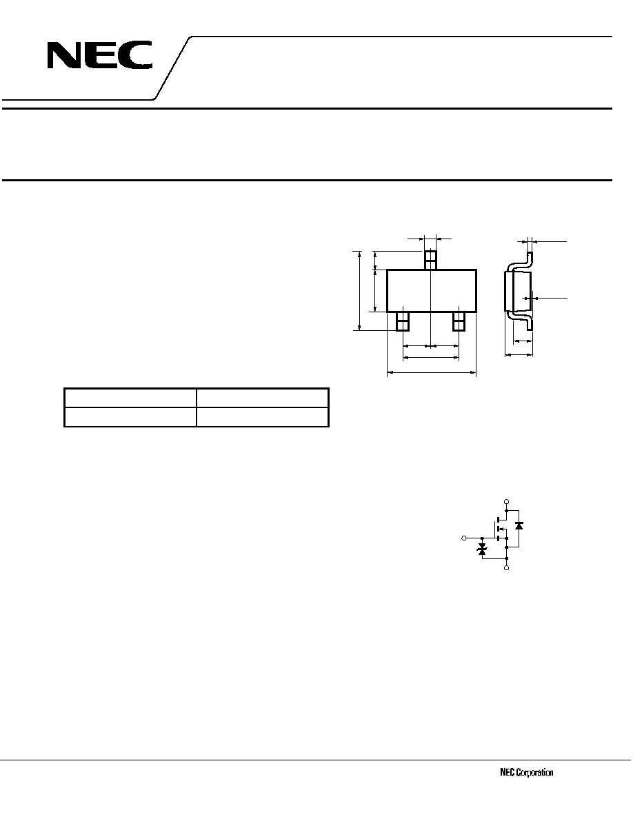
PACKAGE DRAWING (Unit: mm)
0.65
0.9 to 1.1
0 to 0.1
0.16
+0.1
–0.06
2.8
±0.2
1.5
0.95
1
2
3
1.9
2.9 ±0.2
0.4
+0.1
–0.05
0.95
0.65
+0.1 –0.15
1 : Gate
2 : Source
3 : Drain
EQUIVALENT CIRCUIT
Source
Body
Diode
Gate
Protection
Diode
Gate
Drain
相關(guān)PDF資料 |
PDF描述 |
|---|---|
| 2SK3577-A | 3500 mA, 30 V, N-CHANNEL, Si, SMALL SIGNAL, MOSFET |
| 2SK3582TK | 0.34 mA, N-CHANNEL, Si, SMALL SIGNAL, JFET |
| 2SK3582TK-A | 0.34 mA, N-CHANNEL, Si, SMALL SIGNAL, JFET |
| 2SK3582TV | 0.34 mA, N-CHANNEL, Si, SMALL SIGNAL, JFET |
| 2SK3582TV-B | 0.34 mA, N-CHANNEL, Si, SMALL SIGNAL, JFET |
相關(guān)代理商/技術(shù)參數(shù) |
參數(shù)描述 |
|---|---|
| 2SK3576-T1B | 制造商:Renesas Electronics Corporation 功能描述: |
| 2SK3576-T1B-A | 制造商:Renesas Electronics 功能描述:Cut Tape 制造商:Renesas 功能描述:Trans MOSFET N-CH 20V 4A 3-Pin Thin-Type Mini-Mold T/R |
| 2SK3576-T1B-AT | 制造商:Renesas Electronics Corporation 功能描述: |
| 2SK3577-T1B-A | 制造商:Renesas Electronics 功能描述:Cut Tape 制造商:Renesas 功能描述:Trans MOSFET N-CH 30V 3.5A 3-Pin SC-59 |
| 2SK358 | 制造商:Toshiba 功能描述:Bulk |
發(fā)布緊急采購,3分鐘左右您將得到回復。