- 您現(xiàn)在的位置:買賣IC網(wǎng) > PDF目錄33479 > 2SK1449 12 A, 450 V, 0.6 ohm, N-CHANNEL, Si, POWER, MOSFET, TO-3PB PDF資料下載
參數(shù)資料
| 型號(hào): | 2SK1449 |
| 元件分類: | JFETs |
| 英文描述: | 12 A, 450 V, 0.6 ohm, N-CHANNEL, Si, POWER, MOSFET, TO-3PB |
| 封裝: | TO-3PB, 3 PIN |
| 文件頁(yè)數(shù): | 1/4頁(yè) |
| 文件大小: | 109K |
| 代理商: | 2SK1449 |
Any and all SANYO products described or contained herein do not have specifications that can handle
applications that require extremely high levels of reliability, such as life-support systems, aircraft’s
control systems, or other applications whose failure can be reasonably expected to result in serious
physical and/or material damage. Consult with your SANYO representative nearest you before using
any SANYO products described or contained herein in such applications.
SANYO assumes no responsibility for equipment failures that result from using products at values that
exceed, even momentarily, rated values (such as maximum ratings, operating condition ranges,or other
parameters) listed in products specifications of any and all SANYO products described or contained
herein.
N-Channel Silicon MOSFET
Ultrahigh-Speed Switching Applications
Ordering number:EN3452
2SK1449
SANYO Electric Co.,Ltd. Semiconductor Company
TOKYO OFFICE Tokyo Bldg., 1-10, 1 Chome, Ueno, Taito-ku, TOKYO, 110-8534 JAPAN
61099TH (KT)/7151JN (KOTO) X-6827, 8035 No.3452–1/4
Specifications
Absolute Maximum Ratings at Ta = 25C
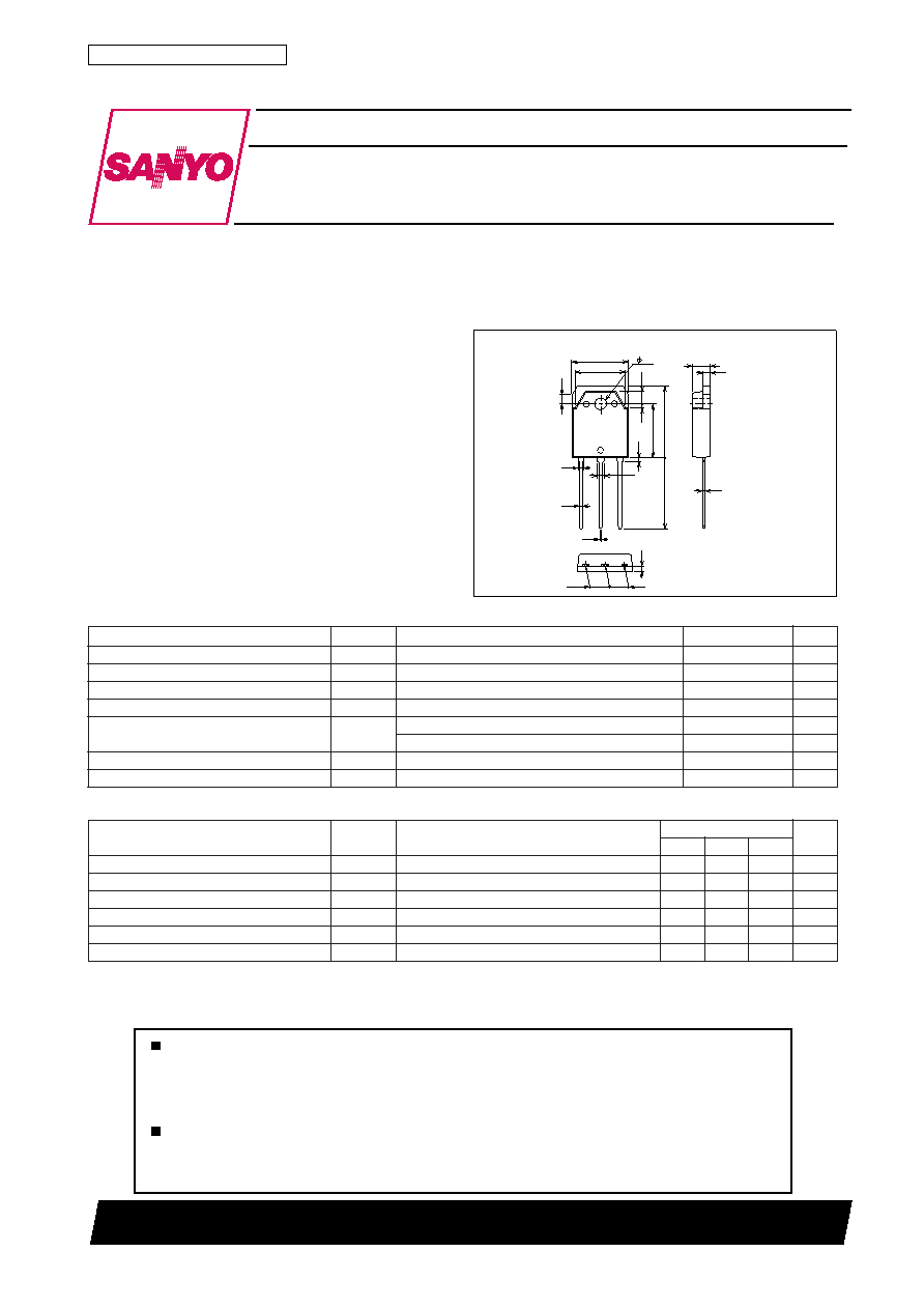
Package Dimensions
unit:mm
2056A
[2SK1449]
Features
Low ON-state resistance.
Ultrahigh-speed switching.
C
Electrical Characteristics at Ta = 25C
1 : Gate
2 : Drain
3 : Source
SANYO : TO-3PB
PW
≤10s, duty cycle≤1%
(Note) Be careful in handling the 2SK1449 because it has no protection diode between gate and source.
Continued on next page.
Tc=25
°C
r
e
t
e
m
a
r
a
Pl
o
b
m
y
Ss
n
o
i
t
i
d
n
o
Cs
g
n
i
t
a
Rt
i
n
U
e
g
a
t
l
o
V
e
c
r
u
o
S
-
o
t
-
n
i
a
r
DV
S
D
0
5
4V
e
g
a
t
l
o
V
e
c
r
u
o
S
-
o
t
-
e
t
a
GV
S
G
0
3
±V
)
C
D
(
t
n
e
r
u
C
n
i
a
r
DID
2
1A
)
e
s
l
u
P
(
t
n
e
r
u
C
n
i
a
r
DI P
D
8
4A
n
o
i
t
a
p
i
s
i
D
r
e
w
o
P
e
l
b
a
w
o
ll
APD
0
2
1W
5
.
2W
e
r
u
t
a
r
e
p
m
e
T
l
e
n
a
h
Ch
c
T
0
5
1
e
r
u
t
a
r
e
p
m
e
T
e
g
a
r
o
t
Sg
t
s
T
0
5
1
+
o
t
5
–
r
e
t
e
m
a
r
a
Pl
o
b
m
y
Ss
n
o
i
t
i
d
n
o
C
s
g
n
i
t
a
R
t
i
n
U
n
i
mp
y
tx
a
m
e
g
a
t
l
o
V
n
w
o
d
k
a
e
r
B
e
c
r
u
o
S
-
o
t
-
n
i
a
r
DV
S
D
)
R
B
(
ID
V
,
A
m
1
=
S
G
0
=0
5
4V
t
n
e
r
u
C
n
i
a
r
D
e
g
a
t
l
o
V
e
t
a
G
-
o
r
e
ZI
S
D
V S
D
V
,
V
0
5
4
=
S
G
0
=0
.
1A
m
t
n
e
r
u
C
e
g
a
k
a
e
L
e
c
r
u
o
S
-
o
t
-
e
t
a
GI
S
G
V S
G
V
,
V
0
3
±
=
S
D
0
=0
0
1
±A
n
e
g
a
t
l
o
V
f
o
t
u
CV
)
f
o
(
S
G
V S
D
I
,
V
0
1
=
D
A
m
1
=0
.
20
.
3V
e
c
n
a
t
i
m
d
A
r
e
f
s
n
a
r
T
d
r
a
w
r
o
F|
s
f
y
|V S
D
I
,
V
0
1
=
D
A
6
=0
.
40
.
8S
e
c
n
a
t
s
i
s
e
R
e
t
a
t
S
-
N
O
e
c
r
u
o
S
-
o
t
-
n
i
a
r
D
c
i
t
a
t
SR
)
n
o
(
S
D
ID
V
,
A
6
=
S
G
V
0
1
=7
4
.
06
.
0
15.6
2.6
3.5
1.2
14.0
1.6
1.0
2.0
0.6
20.0
15.0
1.3
3.2
4.8
2.0
0.6
5.45
1.4
1
2
3
相關(guān)PDF資料 |
PDF描述 |
|---|---|
| 2SK1458 | 0.2 A, 900 V, 70 ohm, N-CHANNEL, Si, POWER, MOSFET, TO-220FI |
| 2SK1460LS | 3.5 A, 900 V, 3.6 ohm, N-CHANNEL, Si, POWER, MOSFET, TO-220FI |
| 2SK1464 | 8 A, 900 V, 1.6 ohm, N-CHANNEL, Si, POWER, MOSFET, TO-3PML |
| 2SK1466 | 16 A, 900 V, 0.8 ohm, N-CHANNEL, Si, POWER, MOSFET, TO-3PBL |
| 2SK1469TP-FA | 8000 mA, 30 V, N-CHANNEL, Si, SMALL SIGNAL, MOSFET |
相關(guān)代理商/技術(shù)參數(shù) |
參數(shù)描述 |
|---|---|
| 2SK1450 | 制造商:SANYO 制造商全稱:Sanyo Semicon Device 功能描述:Very High-Speed Switching Applications |
| 2SK1451 | 制造商:SANYO 制造商全稱:Sanyo Semicon Device 功能描述:Very High-Speed Switching Applications |
| 2SK1452 | 制造商:SANYO 制造商全稱:Sanyo Semicon Device 功能描述:Very High-Speed Switching Applications |
| 2SK1453 | 制造商:SANYO Semiconductor Co Ltd 功能描述:MOSFET N TO-3PML |
| 2SK1453 | 制造商:SANYO Semiconductor Co Ltd 功能描述:MOSFET N TO-3PML |
發(fā)布緊急采購(gòu),3分鐘左右您將得到回復(fù)。