- 您現在的位置:買賣IC網 > PDF目錄371526 > 2SD1741A (PANASONIC CORP) Silicon NPN triple diffusion planar type PDF資料下載
參數資料
| 型號: | 2SD1741A |
| 廠商: | PANASONIC CORP |
| 元件分類: | 功率晶體管 |
| 英文描述: | Silicon NPN triple diffusion planar type |
| 中文描述: | 2 A, 180 V, NPN, Si, POWER TRANSISTOR |
| 封裝: | ROHS COMPLIANT, I-G1, 3 PIN |
| 文件頁數: | 1/2頁 |
| 文件大小: | 49K |
| 代理商: | 2SD1741A |
1
Power Transistors
2SD1741, 2SD1741A
Silicon NPN triple diffusion planar type
For power amplification
For TV vertical deflection output
Complementary to 2SB1171 and 2SB1171A
I
Features
G
High forward current transfer ratio h
FE
which has satisfactory
linearity
G
Low collector to emitter saturation voltage V
CE(sat)
G
I type package enabling direct soldering of the radiating fin to
the printed circuit board, etc. of small electronic equipment.
I
Absolute Maximum Ratings
(T
C
=25C)
Parameter
Collector to
base voltage
Collector to
emitter voltage
Emitter to base voltage
Peak collector current
Collector current
Collector power
dissipation
Junction temperature
Storage temperature
Symbol
V
CBO
V
CEO
V
EBO
I
CP
I
C
P
C
T
j
T
stg
Ratings
200
200
150
180
6
3
2
15
1.3
150
–55 to +150
Unit
V
V
V
A
A
W
C
C
2SD1741
2SD1741A
2SD1741
2SD1741A
T
C
=25
°
C
Ta=25
°
C
I
Electrical Characteristics
(T
C
=25C)
Parameter
Collector cutoff current
Emitter cutoff current
Collector to base voltage
Collector to emitter
voltage
Emitter to base voltage
Forward current transfer ratio
Base to emitter voltage
Collector to emitter saturation voltage
Transition frequency
Symbol
I
CBO
I
EBO
V
CBO
V
CEO
V
EBO
h
FE1*
h
FE2
V
BE
V
CE(sat)
f
T
Conditions
V
CB
= 200V, I
E
= 0
V
EB
= 4V, I
C
= 0
I
C
= 50
μ
A, I
E
= 0
I
C
= 5mA, I
B
= 0
I
E
= 500
μ
A, I
C
= 0
V
CE
= 10V, I
C
= 150mA
V
CE
= 10V, I
C
= 400mA
V
CE
= 10V, I
C
= 400mA
I
C
= 500mA, I
B
= 50mA
V
CE
= 10V, I
C
= 0.5A, f = 1MHz
min
200
150
180
6
60
50
typ
20
max
50
50
240
1
1
Unit
μ
A
μ
A
V
V
V
V
V
MHz
2SD1741
2SD1741A
*
h
FE1
Rank classification
Rank
Q
P
h
FE1
60 to 140
100 to 240
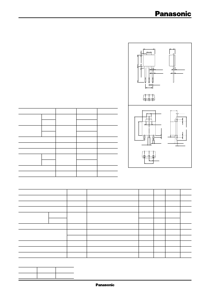
Unit: mm
1:Base
2:Collector
3:Emitter
I Type Package
Unit: mm
1:Base
2:Collector
3:Emitter
I Type Package (Y)
7
±
0
7.0
±
0.3
3.0
±
0.2
3.5
±
0.2
1
+
–
0
±
0
1
±
0
4.6
±
0.4
2
1
3
1.1
±
0.1
0.75
±
0.1
2.3
±
0.2
0.85
±
0.1
0.4
±
0.1
7.0
±
0.3
0.75
±
0.1
2.3
±
0.2
4.6
±
0.4
1.1
±
0.1
1
±
0
7
±
0
2.0
±
0.2
0.9
±
0.1
0 to 0.15
3.5
±
0.2
2
±
0
1
1
2
±
0
3.0
±
0.2
1
1
2
3
0 to 0.15
2.5
0.5 max.
相關PDF資料 |
PDF描述 |
|---|---|
| 2SD1742 | Silicon NPN triple diffusion planar type |
| 2SD1742A | Silicon NPN triple diffusion planar type |
| 2SD1743 | Silicon NPN triple diffusion planar type |
| 2SD1743A | Silicon NPN triple diffusion planar type |
| 2SD1744 | Silicon NPN epitaxial planar type |
相關代理商/技術參數 |
參數描述 |
|---|---|
| 2SD1748 | 制造商:Distributed By MCM 功能描述:SUB ONLY HITACHI TRANS. I-TYPE 60V 2A 15W BCE SURFACE MOUNT |
| 2SD175 | 制造商:Distributed By MCM 功能描述:SUB ONLY TRANSISTOR TO-3 100V 5A 50W BEC |
| 2SD1755 | 制造商:Panasonic Industrial Company 功能描述:TRANSISTOR |
| 2SD1757 | 制造商:Panasonic Industrial Company 功能描述:TRANSISTOR |
| 2SD1757K | 制造商:Panasonic Industrial Company 功能描述:TRANSISTOR |
發(fā)布緊急采購,3分鐘左右您將得到回復。