- 您現(xiàn)在的位置:買(mǎi)賣(mài)IC網(wǎng) > PDF目錄49934 > 2SC4031 0.02 A, 900 V, NPN, Si, POWER TRANSISTOR PDF資料下載
參數(shù)資料
| 型號(hào): | 2SC4031 |
| 元件分類(lèi): | 功率晶體管 |
| 英文描述: | 0.02 A, 900 V, NPN, Si, POWER TRANSISTOR |
| 封裝: | TO-220MF, 3 PIN |
| 文件頁(yè)數(shù): | 1/4頁(yè) |
| 文件大?。?/td> | 53K |
| 代理商: | 2SC4031 |
Any and all SANYO products described or contained herein do not have specifications that can handle
applications that require extremely high levels of reliability, such as life-support systems, aircraft’s
control systems, or other applications whose failure can be reasonably expected to result in serious
physical and/or material damage. Consult with your SANYO representative nearest you before using
any SANYO products described or contained herein in such applications.
SANYO assumes no responsibility for equipment failures that result from using products at values that
exceed, even momentarily, rated values (such as maximum ratings, operating condition ranges,or other
parameters) listed in products specifications of any and all SANYO products described or contained
herein.
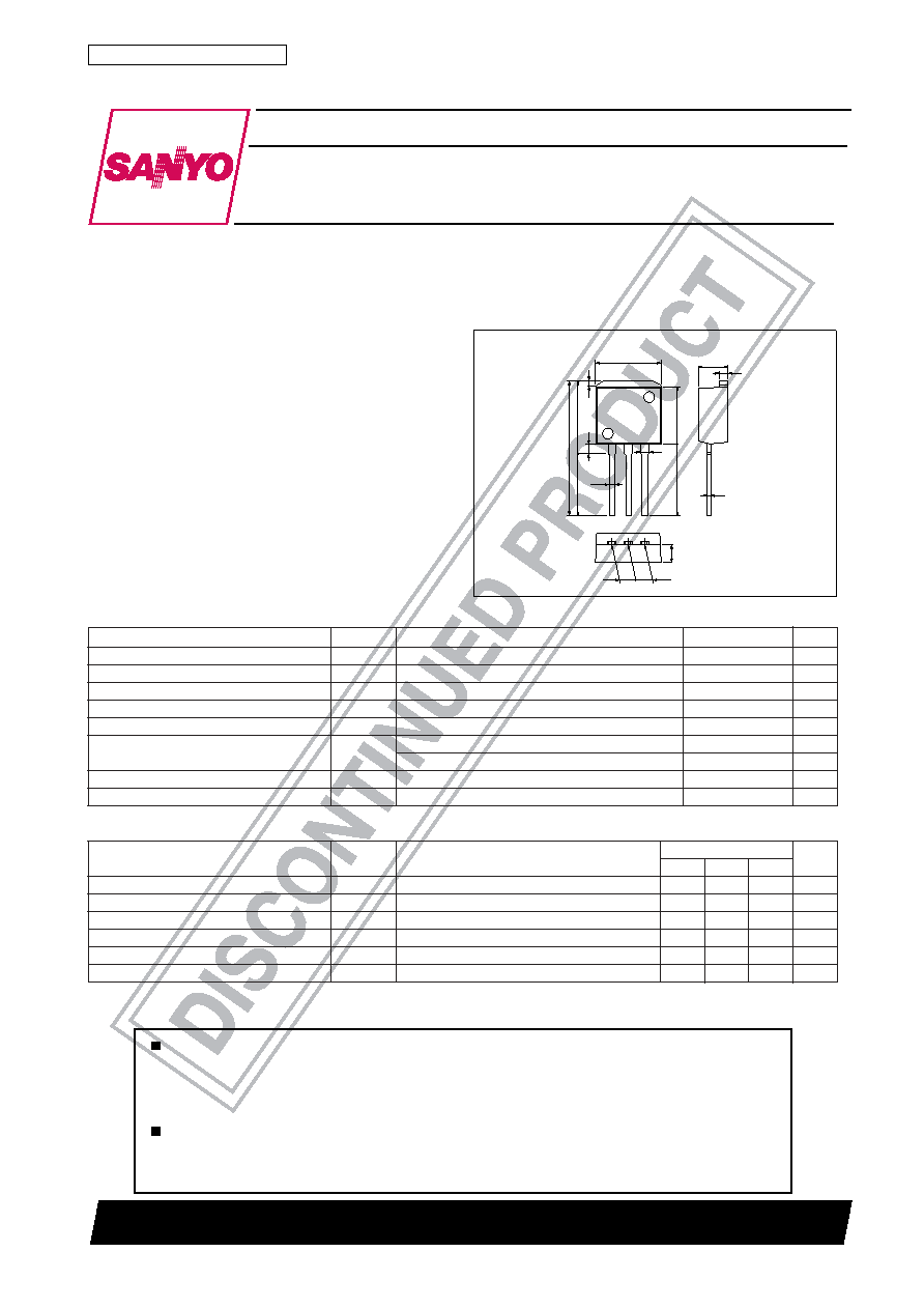
NPN Triple Diffused Planar Silicon Transistor
900V/20mA Switching Applications
Ordering number:ENN2478B
2SC4031
SANYO Electric Co.,Ltd. Semiconductor Company
TOKYO OFFICE Tokyo Bldg., 1-10, 1 Chome, Ueno, Taito-ku, TOKYO, 110-8534 JAPAN
70804TN (PC)/D1598HA (KT)/D051MH, (KOTO) No.2478–1/4
Specifications
Absolute Maximum Ratings at Ta = 25C
Package Dimensions
unit:mm
2049C
[2SC4031]
Features
High breakdown voltage (VCEO min=900V).
Small Output Capacitance (Cob typ=1.6pF).
Wide ASO (adoption of MBIT process).
High reliability (adoption of HVP process).
C
Electrical Characteristics at Ta = 25C
1 : Base
2 : Collector
3 : Emitter
SANYO : TO-220MF
Tc=25C
r
e
t
e
m
a
r
a
Pl
o
b
m
y
Ss
n
o
i
t
i
d
n
o
Cs
g
n
i
t
a
Rt
i
n
U
e
g
a
t
l
o
V
e
s
a
B
-
o
t
-
r
o
t
c
e
ll
o
CV
O
B
C
0
2V
e
g
a
t
l
o
V
r
e
t
i
m
E
-
o
t
-
r
o
t
c
e
ll
o
CV
O
E
C
0
9V
e
g
a
t
l
o
V
e
s
a
B
-
o
t
-
r
e
t
i
m
EV
O
B
E
5V
t
n
e
r
u
C
r
o
t
c
e
ll
o
CIC
0
2A
m
)
e
s
l
u
P
(
t
n
e
r
u
C
r
o
t
c
e
ll
o
CI P
C
0
6A
m
n
o
i
t
a
p
i
s
i
D
r
o
t
c
e
ll
o
CPC
5
6
.
1W
2
.
1W
e
r
u
t
a
r
e
p
m
e
T
n
o
i
t
c
n
u
Jj
T
0
5
1
e
r
u
t
a
r
e
p
m
e
T
e
g
a
r
o
t
Sg
t
s
T
0
5
1
+
o
t
5
–
r
e
t
e
m
a
r
a
Pl
o
b
m
y
Ss
n
o
i
t
i
d
n
o
C
s
g
n
i
t
a
R
t
i
n
U
n
i
mp
y
tx
a
m
t
n
e
r
u
C
f
o
t
u
C
r
o
t
c
e
ll
o
CI
O
B
C
V B
C
I
,
V
0
9
=
E 0
=1
A
t
n
e
r
u
C
f
o
t
u
C
r
e
t
i
m
EI
O
B
E
V B
E
I
,
V
4
=
C 0
=1
A
n
i
a
G
t
n
e
r
u
C
Dh E
F
V E
C
I
,
V
5
=
C
A
m
1
=0
20
50
2
1
t
c
u
d
o
r
P
h
t
d
i
w
d
n
a
B
-
n
i
a
GfT
V E
C
I
,
V
0
1
=
C
A
m
1
=6
z
H
M
e
g
a
t
l
o
V
n
o
i
t
a
r
u
t
a
S
r
e
t
i
m
E
-
o
t
-
r
o
t
c
e
ll
o
CV
)
t
a
s
(
E
C
IC
I
,
A
m
2
=
B
A
0
4
=5
V
e
g
a
t
l
o
V
n
o
i
t
a
r
u
t
a
S
r
e
t
i
m
E
-
o
t
-
e
s
a
BV
)
t
a
s
(
E
B
IC
I
,
A
m
2
=
B
A
0
4
=2
V
10.2
20.9
11.5
9.4
0.8
1.6
1.2
0.9
11.0
8.8
4.5
1.3
0.4
2.55
2.7
12
3
Continued on next page.
相關(guān)PDF資料 |
PDF描述 |
|---|---|
| 2SC4037TL2/Q | 500 mA, 32 V, NPN, Si, SMALL SIGNAL TRANSISTOR |
| 2SC4044S/LP | UHF BAND, Si, NPN, RF SMALL SIGNAL TRANSISTOR |
| 2SC2926T93/MQ | UHF BAND, Si, NPN, RF SMALL SIGNAL TRANSISTOR, TO-92 |
| 2SC4044S/Q | UHF BAND, Si, NPN, RF SMALL SIGNAL TRANSISTOR |
| 2SC3377/PR | 1000 mA, 32 V, NPN, Si, SMALL SIGNAL TRANSISTOR, TO-92 |
相關(guān)代理商/技術(shù)參數(shù) |
參數(shù)描述 |
|---|---|
| 2SC4032 | 制造商:Distributed By MCM 功能描述:SUB ONLY TRANSISTOR FTL40V .3A .3W ECB |
| 2SC4034 | 制造商:Distributed By MCM 功能描述:SUB ONLY TRANSISTOR ATV80V .05A .15W ECB |
| 2SC4034Q | 制造商:未知廠家 制造商全稱(chēng):未知廠家 功能描述:TRANSISTOR | BJT | NPN | 80V V(BR)CEO | 50MA I(C) | SC-71VAR |
| 2SC4034R | 制造商:未知廠家 制造商全稱(chēng):未知廠家 功能描述:TRANSISTOR | BJT | NPN | 80V V(BR)CEO | 50MA I(C) | SC-71VAR |
| 2SC4034S | 制造商:未知廠家 制造商全稱(chēng):未知廠家 功能描述:TRANSISTOR | BJT | NPN | 80V V(BR)CEO | 50MA I(C) | SC-71VAR |
發(fā)布緊急采購(gòu),3分鐘左右您將得到回復(fù)。