- 您現(xiàn)在的位置:買賣IC網(wǎng) > PDF目錄33333 > 2SB1118-U 700 mA, 15 V, PNP, Si, SMALL SIGNAL TRANSISTOR PDF資料下載
參數(shù)資料
| 型號: | 2SB1118-U |
| 元件分類: | 小信號晶體管 |
| 英文描述: | 700 mA, 15 V, PNP, Si, SMALL SIGNAL TRANSISTOR |
| 封裝: | PCP, 3 PIN |
| 文件頁數(shù): | 1/3頁 |
| 文件大小: | 115K |
| 代理商: | 2SB1118-U |
SANYO Electric Co.,Ltd. Semiconductor Bussiness Headquaters
TOKYO OFFICE Tokyo Bldg., 1-10, 1 Chome, Ueno, Taito-ku, TOKYO, 110-8534 JAPAN
Any and all SANYO products described or contained herein do not have specifications that can handle
applications that require extremely high levels of reliability, such as life-support systems, aircraft’s
control systems, or other applications whose failure can be reasonably expected to result in serious
physical and/or material damage. Consult with your SANYO representative nearest you before using
any SANYO products described or contained herein in such applications.
SANYO assumes no responsibility for equipment failures that result from using products at values that
exceed, even momentarily, rated values (such as maximum ratings, operating condition ranges,or other
parameters) listed in products specifications of any and all SANYO products described or contained
herein.
PNP/NPN Epitaxial Planar Silicon Transistors
Low-Voltage High-Current Amplifier,
Muting Applications
Ordering number:1784B
2SB1118/2SD1618
92098HA (KT)/4017KI/0216AT/2065MY, TS No.1784–1/3
r
e
t
e
m
a
r
a
Pl
o
b
m
y
Ss
n
o
i
t
i
d
n
o
Cs
g
n
i
t
a
Rt
i
n
U
e
g
a
t
l
o
V
e
s
a
B
-
o
t
-
r
o
t
c
e
ll
o
CV
O
B
C
0
2
)
–
(V
e
g
a
t
l
o
V
r
e
t
i
m
E
-
o
t
-
r
o
t
c
e
ll
o
CV
O
E
C
5
1
)
–
(V
e
g
a
t
l
o
V
e
s
a
B
-
o
t
-
r
e
t
i
m
EV
O
B
E
5
)
–
(V
t
n
e
r
u
C
r
o
t
c
e
ll
o
CIC
7
.
0
)
–
(A
)
e
s
l
u
P
(
t
n
e
r
u
C
r
o
t
c
e
ll
o
CI P
C
5
.
1
)
–
(A
n
o
i
t
a
p
i
s
i
D
r
o
t
c
e
ll
o
CPC
0
5W
m
3
.
1W
e
r
u
t
a
r
e
p
m
e
T
n
o
i
t
c
n
u
Jj
T
0
5
1
e
r
u
t
a
r
e
p
m
e
T
e
g
a
r
o
t
Sg
t
s
T
0
5
1
+
o
t
5
–
( ) : 2SB1118
Specifications
Absolute Maximum Ratings at Ta = 25C
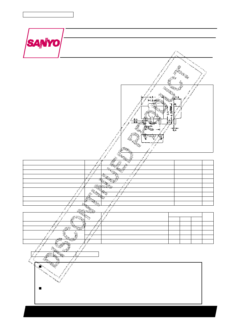
Package Dimensions
unit:mm
2038
[2SB1118/2SD1618]
Features
Low collector-to-emitter saturation voltage.
Very small size making it easy to provide high-
density, small-sized hybrid IC’s.
C
Electrical Characteristics at Ta = 25C
E : Emitter
C : Collector
B : Base
SANYO : PCP
(Bottom view)
Mounted on ceramic board (250mm
2
×0.8mm)
r
e
t
e
m
a
r
a
Pl
o
b
m
y
Ss
n
o
i
t
i
d
n
o
C
s
g
n
i
t
a
R
t
i
n
U
n
i
mp
y
tx
a
m
t
n
e
r
u
C
f
o
t
u
C
r
o
t
c
e
ll
o
CI
O
B
C
V B
C
I
,
V
5
1
)
–
(
=
E 0
=1
.
0
)
–
(A
t
n
e
r
u
C
f
o
t
u
C
r
e
t
i
m
EI
O
B
E
V B
E
I
,
V
4
)
–
(
=
C 0
=1
.
0
)
–
(A
n
i
a
G
t
n
e
r
u
C
Dh E
F 1V E
C
I
,
V
2
)
–
(
=
C
A
m
0
5
)
–
(
=
*
0
4
1*
0
6
5
h E
F 2V E
C
I
,
V
2
)
–
(
=
C
A
m
0
5
)
–
(
=
0
6
t
c
u
d
o
r
P
h
t
d
i
w
d
n
a
B
-
n
i
a
GfT
V E
C
I
,
V
0
1
)
–
(
=
C
A
m
0
5
)
–
(
=
0
5
2z
H
M
* ; The 2SB1118/2SD1618 are classified by 50mA hFE as follows :
Marking 2SB1118 : BA
2SD1618 : DA
hFE rank : S, T, U
0
8
2
S
0
4
10
0
4
T
0
20
6
5
U
0
8
2
相關(guān)PDF資料 |
PDF描述 |
|---|---|
| 2SD1618S | 700 mA, 15 V, NPN, Si, SMALL SIGNAL TRANSISTOR |
| 2SD1618-T | 700 mA, 15 V, NPN, Si, SMALL SIGNAL TRANSISTOR |
| 2SD1618-S | 700 mA, 15 V, NPN, Si, SMALL SIGNAL TRANSISTOR |
| 2SD1618U | 700 mA, 15 V, NPN, Si, SMALL SIGNAL TRANSISTOR |
| 2SB1118T | 700 mA, 15 V, PNP, Si, SMALL SIGNAL TRANSISTOR |
相關(guān)代理商/技術(shù)參數(shù) |
參數(shù)描述 |
|---|---|
| 2SB1119 | 制造商:Distributed By MCM 功能描述:SUB ONLY SANYO TRANS. SC-62-25V -1A .5W ECB SURFACE MT |
| 2SB1119R | 制造商:未知廠家 制造商全稱:未知廠家 功能描述:TRANSISTOR | BJT | PNP | 25V V(BR)CEO | 1A I(C) | SOT-89 |
| 2SB1119S | 制造商:未知廠家 制造商全稱:未知廠家 功能描述:TRANSISTOR | BJT | PNP | 25V V(BR)CEO | 1A I(C) | SOT-89 |
| 2SB1119S-TD-E | 制造商:Sanyo Semi. 功能描述: 制造商:SANYO Semiconductor Co Ltd 功能描述: |
| 2SB1119T | 制造商:未知廠家 制造商全稱:未知廠家 功能描述:TRANSISTOR | BJT | PNP | 25V V(BR)CEO | 1A I(C) | SOT-89 |
發(fā)布緊急采購,3分鐘左右您將得到回復(fù)。