- 您現(xiàn)在的位置:買賣IC網(wǎng) > PDF目錄30445 > 2N5433 (CALOGIC LLC) 400 mA, N-CHANNEL, Si, SMALL SIGNAL, JFET, TO-52 PDF資料下載
參數(shù)資料
| 型號: | 2N5433 |
| 廠商: | CALOGIC LLC |
| 元件分類: | 小信號晶體管 |
| 英文描述: | 400 mA, N-CHANNEL, Si, SMALL SIGNAL, JFET, TO-52 |
| 封裝: | HERMETIC SEALED PACKAGE-3 |
| 文件頁數(shù): | 1/2頁 |
| 文件大?。?/td> | 30K |
| 代理商: | 2N5433 |
N-Channel JFET Switch
2N5432 – 2N5434
FEATURES
Low rds(on)
Excellent Switching
Low Cutoff Current
ABSOLUTE MAXIMUM RATINGS
(TA = 25
oC unless otherwise noted)
Gate-Source Voltage . . . . . . . . . . . . . . . . . . . . . . . . . . . . -25V
Gate-Drain Voltage . . . . . . . . . . . . . . . . . . . . . . . . . . . . . -25V
Gate Current . . . . . . . . . . . . . . . . . . . . . . . . . . . . . . . . 100mA
Drain Current . . . . . . . . . . . . . . . . . . . . . . . . . . . . . . . . 400mA
Storage Temperature Range . . . . . . . . . . . . . -65
oC to +200oC
Operating Temperature Range . . . . . . . . . . . -55
oC to +150oC
Lead Temperature (Soldering, 10sec) . . . . . . . . . . . . . +300
oC
Power Dissipation . . . . . . . . . . . . . . . . . . . . . . . . . . . . 300mW
Derate above 25
oC . . . . . . . . . . . . . . . . . . . . . . . 2.3mW/oC
NOTE: Stresses above those listed under "Absolute Maximum
Ratings" may cause permanent damage to the device. These are
stress ratings only and functional operation of the device at these or
any other conditions above those indicated in the operational sections
of the specifications is not implied. Exposure to absolute maximum
rating conditions for extended periods may affect device reliability.
ORDERING INFORMATION
Part
Package
Temperature Range
2N5432-34
Hermetic TO-52
-55
oC to +150oC
X2N5432-34 Sorted Chips in Carriers
-55
oC to +150oC
LLC
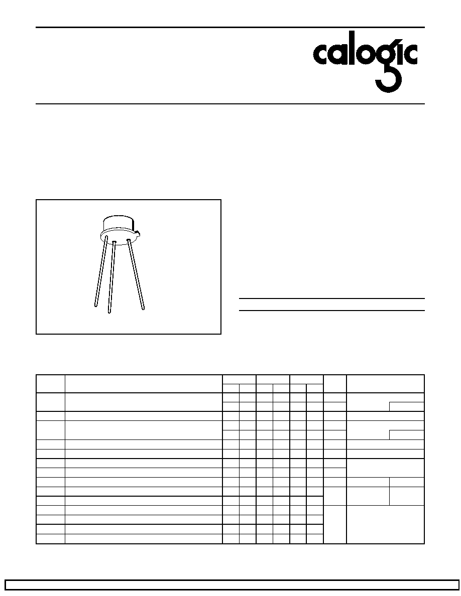
PIN CONFIGURATION
D
S
(TO-52)
G, C
ELECTRICAL CHARACTERISTICS (TA = 25
oC unless otherwise specified)
SYMBOL
PARAMETER
2N5432
2N5433
2N5434
UNITS
TEST CONDITIONS
MIN MAX MIN MAX MIN MAX
IGSS
Gate Reverse Current
-200
pA
VGS = -15V, VDS = 0
-200
nA
TA = 150
oC
BVGSS
Gate-Source Breakdown Voltage
-25
V
IG = -1
A, VDS = 0
ID(off)
Drain Cutoff Current
200
pA
VDS = 5V, VGS = -10V
200
nA
TA = 150
oC
VGS(off)
Gate-Source Cutoff Voltage
-4
-10
-3
-9
-1
-4
V
VDS = 5V, ID = 3nA
IDSS
Saturation Drain Current (Note 1)
150
100
30
mA
VDS = 15V, VGS = 0
rDS(on)
Static Drain-Source ON Resistance
2
5
7
10
ohm
VGS = 0, ID = 10mA
VDS(on)
Drain-Source ON Voltage
50
70
100
mV
rds(on)
Drain-Source ON Resistance
5
7
10
ohm
VGS = 0, ID = 0 f = 1kHz
Ciss
Common-Source Input Capacitance (Note2)
30
pF
VDS = 0,
VGS = -10 V
f = 1MHz
Crss
Common-Source Reverse Transfer Capacitance (Note 2)
15
td
Turn-ON Delay Time (Note 2)
4
ns
VDD = 1.5V,
VGS(on) = 0,
VGS(off) = -12V,
ID(on) = 10mA
tr
Rise Time (Note 2)
1
toff
Turn-OFF Delay Time (Note 2)
6
tf
Fall Time (Note 2)
30
NOTES: 1. Pulse test required, pulsewidth 300
s, duty cycle ≤3%.
2. For design reference only, not 100% tested.
5018
CALOGIC LLC, 237 WHITNEY PLACE, FREMONT, CA 94539, 510-656-2900 PHONE, 510-651-1076 FAX
DS009 REV A
相關(guān)PDF資料 |
PDF描述 |
|---|---|
| 2N5432 | 400 mA, N-CHANNEL, Si, SMALL SIGNAL, JFET, TO-52 |
| 2N5457D75Z | N-CHANNEL, Si, SMALL SIGNAL, JFET, TO-92 |
| 2N5457D26Z | N-CHANNEL, Si, SMALL SIGNAL, JFET, TO-92 |
| 2N5457D27Z | N-CHANNEL, Si, SMALL SIGNAL, JFET, TO-92 |
| 2N5458D75Z | N-CHANNEL, Si, SMALL SIGNAL, JFET, TO-92 |
相關(guān)代理商/技術(shù)參數(shù) |
參數(shù)描述 |
|---|---|
| 2N5433-2 | 制造商:Vishay Siliconix 功能描述:TRANS JFET N-CH 3PIN TO-52 - Bulk |
| 2N5433-DIE | 制造商:Vishay Siliconix 功能描述: |
| 2N5433-E3 | 功能描述:JFET 25V 10pA RoHS:否 制造商:ON Semiconductor 晶體管極性:N-Channel 漏極電流(Vgs=0 時(shí)的 Idss):50 mA 漏源電壓 VDS:15 V 閘/源擊穿電壓: 漏極連續(xù)電流:50 mA 配置: 安裝風(fēng)格: 封裝 / 箱體:SC-59 封裝:Reel |
| 2N5434 | 功能描述:JFET 25V 10pA RoHS:否 制造商:ON Semiconductor 晶體管極性:N-Channel 漏極電流(Vgs=0 時(shí)的 Idss):50 mA 漏源電壓 VDS:15 V 閘/源擊穿電壓: 漏極連續(xù)電流:50 mA 配置: 安裝風(fēng)格: 封裝 / 箱體:SC-59 封裝:Reel |
| 2N5434-2 | 功能描述:JFET FIELD EFFECT TRANS RoHS:否 制造商:ON Semiconductor 晶體管極性:N-Channel 漏極電流(Vgs=0 時(shí)的 Idss):50 mA 漏源電壓 VDS:15 V 閘/源擊穿電壓: 漏極連續(xù)電流:50 mA 配置: 安裝風(fēng)格: 封裝 / 箱體:SC-59 封裝:Reel |
發(fā)布緊急采購,3分鐘左右您將得到回復(fù)。