- 您現(xiàn)在的位置:買賣IC網(wǎng) > PDF目錄371438 > 29C256 (Atmel Corp.) 256K 32K x 8 5-volt Only CMOS Flash Memory PDF資料下載
參數(shù)資料
| 型號: | 29C256 |
| 廠商: | Atmel Corp. |
| 英文描述: | 256K 32K x 8 5-volt Only CMOS Flash Memory |
| 中文描述: | 256K 32K的× 8 5伏只有閃存的CMOS |
| 文件頁數(shù): | 2/17頁 |
| 文件大小: | 343K |
| 代理商: | 29C256 |

2
AT29C256
0046P–FLASH–10/04
To allow for simple in-system reprogrammability, the AT29C256 does not require high
input voltages for programming. Five-volt-only commands determine the operation of
the device. Reading data out of the device is similar to reading from a static RAM.
Reprogramming the AT29C256 is performed on a page basis; 64 bytes of data are
loaded into the device and then simultaneously programmed. The contents of the entire
device may be erased by using a six-byte software code (although erasure before pro-
gramming is not needed).
During a reprogram cycle, the address locations and 64 bytes of data are internally
latched, freeing the address and data bus for other operations. Following the initiation of
a program cycle, the device will automatically erase the page and then program the
latched data using an internal control timer. The end of a program cycle can be detected
by DATA polling of I/O7. Once the end of a program cycle has been detected a new
access for a read, program or chip erase can begin.
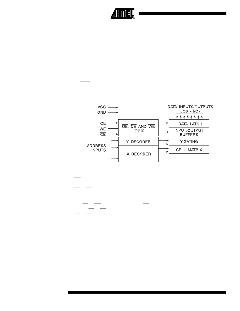
Block Diagram
Device Operation
READ:
WE is high, the data stored at the memory location determined by the address pins
is asserted on the outputs. The outputs are put in the high impedance state whenever
CE or OE is high. This dual-line control gives designers flexibility in preventing bus
contention.
The AT29C256 is accessed like a static RAM. When CE and OE are low and
BYTE LOAD:
with CE or WE low (respectively) and OE high. The address is latched on the falling
edge of CE or WE, whichever occurs last. The data is latched by the first rising edge of
CE or WE. Byte loads are used to enter the 64 bytes of a page to be programmed or the
software codes for data protection and chip erasure.
A byte load is performed by applying a low pulse on the WE or CE input
相關(guān)PDF資料 |
PDF描述 |
|---|---|
| 29C48 | Telecommunication IC |
| 29C512 | 512K 64K x 8 5-volt Only CMOS Flash Memory |
| 29C516E | 97-3106A14S-5S |
| 29C532E | 5-Pin, Multiple-Input, Programmable Reset ICs |
| 29C93 | ISDN, Other/Special/Miscellaneous |
相關(guān)代理商/技術(shù)參數(shù) |
參數(shù)描述 |
|---|---|
| 29C25615JC | 制造商: 功能描述: 制造商:undefined 功能描述: |
| 29C256-15JC | 制造商: 功能描述: 制造商:undefined 功能描述: |
| 29C42 | 制造商:未知廠家 制造商全稱:未知廠家 功能描述:Protocol Controller |
| 29C462 | 制造商:未知廠家 制造商全稱:未知廠家 功能描述:Communications Controller |
| 29C48 | 制造商:未知廠家 制造商全稱:未知廠家 功能描述:Telecommunication IC |
發(fā)布緊急采購,3分鐘左右您將得到回復(fù)。