- 您現(xiàn)在的位置:買賣IC網(wǎng) > PDF目錄298293 > 28C17AT-15/VS 2K X 8 EEPROM 5V, 150 ns, PDSO28 PDF資料下載
參數(shù)資料
| 型號: | 28C17AT-15/VS |
| 元件分類: | PROM |
| 英文描述: | 2K X 8 EEPROM 5V, 150 ns, PDSO28 |
| 封裝: | 8 X 13.40 MM, VSOP-28 |
| 文件頁數(shù): | 6/8頁 |
| 文件大小: | 100K |
| 代理商: | 28C17AT-15/VS |
28C17A
DS11127F-page 6
1994 Microchip Technology Inc.
2.0
DEVICE OPERATION
The Microchip Technology Inc. 28C17A has four basic
modes of operation—read, standby, write inhibit, and
byte write—as outlined in the following table.
2.1
Read Mode
The 28C17A has two control functions, both of which
must be logically satised in order to obtain data at the
outputs. Chip enable (CE) is the power control and
should be used for device selection. Output Enable
(OE) is the output control and is used to gate data to
the output pins independent of device selection.
Assuming that addresses are stable, address access
time (tACC) equal to the delay from CE to output (tCE).
Data is available at the output tOE after the falling edge
of OE, assuming that CE has been low and addresses
have been stable for at least tACC-tOE.
2.2
Standby Mode
The 28C17A is placed in the standby mode by applying
a high signal to the CE input. When in the standby
mode, the outputs are in a high impedance state, inde-
pendent of the OE input.
2.3
Data Protection
In order to ensure data integrity, especially during criti-
cal power-up and power-down transitions, the following
enhanced data protection circuits are incorporated:
First, an internal VCC detect (3.3 volts typical) will inhibit
the initiation of non-volatile programming operation
when VCC is less than the VCC detect circuit trip.
Second, there is a WE ltering circuit that prevents WE
pulses of less than 10 ns duration from initiating a write
cycle.
Third, holding WE or CE high or OE low, inhibits a write
cycle during power-on and power-off (VCC).
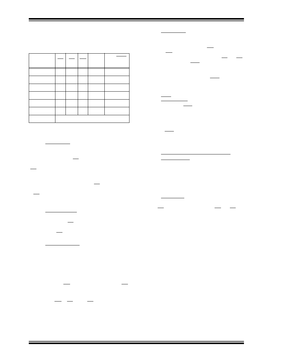
Operation
Mode
CE
OE
WE
I/O
Rdy/Busy
(1)
Read
L
H
DOUT
H
Standby
H
X
High Z
H
Write Inhibit
H
X
High Z
H
Write Inhibit
X
L
X
High Z
H
Write Inhibit
X
H
High Z
H
Byte Write
L
H
L
DIN
L
Byte Clear
Automatic Before Each “Write”
Note 1: Open drain output.
Note 2: X = Any TTL level.
2.4
Write Mode
The 28C17A has a write cycle similar to that of a Static
RAM. The write cycle is completely self-timed and ini-
tiated by a low going pulse on the WE pin. On the fall-
ing edge of WE, the address information is latched. On
rising edge, the data and the control pins (CE and OE)
are latched. The Ready/Busy pin goes to a logic low
level indicating that the 28C17A is in a write cycle which
signals the microprocessor host that the system bus is
free for other activity. When Ready/Busy goes back to
a high, the 28C17A has completed writing and is ready
to accept another cycle.
2.5
Data Polling
The 28C17A features Data polling to signal the comple-
tion of a byte write cycle.
During a write cycle, an
attempted read of the last byte written results in the
data complement of I/O7 (I/O0 to I/O6 are indetermin-
able). After completion of the write cycle, true data is
available. Data polling allows a simple read/compare
operation to determine the status of the chip eliminat-
ing the need for external hardware.
2.6
Electronic Signature for Device
Identication
An extra row of 32 bytes of EEPROM memory is avail-
able to the user for device identication. By raising A9
to 12V
±0.5V and using address locations 7EO to 7FF,
the additional bytes can be written to or read from in the
same manner as the regular memory array.
2.7
Chip Clear
All data may be cleared to 1's in a chip clear cycle by
raising OE to 12 volts and bringing the WE and CE low.
This procedure clears all data, except for the extra row.
相關(guān)PDF資料 |
PDF描述 |
|---|---|
| 28C64AX-20I/K | 8K X 8 EEPROM 5V, 200 ns, CQCC32 |
| 28JS161-2 | PANEL MOUNT, CABLE TERMINATED, FEMALE, BNC CONNECTOR, CLAMP, JACK |
| 28P156-1 | CABLE TERMINATED, MALE-FEMALE, RF STRAIGHT ADAPTER, PLUG-RECEPTACLE |
| 2910A | MU-LAW, PCM CODEC |
| 292317-1 | 4 CONTACT(S), FEMALE, RIGHT ANGLE TELECOM AND DATACOM CONNECTOR, SOLDER, RECEPTACLE |
相關(guān)代理商/技術(shù)參數(shù) |
參數(shù)描述 |
|---|---|
| 28C17AT-25I/SOJ31 | 制造商:Microchip Technology Inc 功能描述:2K X 8 EEPROM 5V, 250 NS, PDSO28 |
| 28-C182-00 | 功能描述:IC 與器件插座 LOCK/EJECT DIP SCKT SURFACE MOUNT 28 PIN RoHS:否 制造商:Molex 產(chǎn)品:LGA Sockets 節(jié)距:1.02 mm 排數(shù): 位置/觸點(diǎn)數(shù)量:2011 觸點(diǎn)電鍍:Gold 安裝風(fēng)格:SMD/SMT 端接類型:Solder 插座/封裝類型:LGA 2011 工作溫度范圍:- 40 C to + 100 C |
| 28-C182-10 | 功能描述:IC 與器件插座 28P LOCK/EJECT SOCK RoHS:否 制造商:Molex 產(chǎn)品:LGA Sockets 節(jié)距:1.02 mm 排數(shù): 位置/觸點(diǎn)數(shù)量:2011 觸點(diǎn)電鍍:Gold 安裝風(fēng)格:SMD/SMT 端接類型:Solder 插座/封裝類型:LGA 2011 工作溫度范圍:- 40 C to + 100 C |
| 28-C182-10 | 制造商:Aries Electronics Inc 功能描述:IC SOCKET DIL LOCK/EJECT |
| 28-C182-11 | 功能描述:IC 與器件插座 28P LOCK/EJECT SKT RoHS:否 制造商:Molex 產(chǎn)品:LGA Sockets 節(jié)距:1.02 mm 排數(shù): 位置/觸點(diǎn)數(shù)量:2011 觸點(diǎn)電鍍:Gold 安裝風(fēng)格:SMD/SMT 端接類型:Solder 插座/封裝類型:LGA 2011 工作溫度范圍:- 40 C to + 100 C |
發(fā)布緊急采購,3分鐘左右您將得到回復(fù)。