- 您現(xiàn)在的位置:買賣IC網(wǎng) > PDF目錄371428 > 27L2AI (Texas Instruments, Inc.) LinCMOSE PRECISION DUAL OPERATIONAL AMPLIFIERS PDF資料下載
參數(shù)資料
| 型號(hào): | 27L2AI |
| 廠商: | Texas Instruments, Inc. |
| 英文描述: | LinCMOSE PRECISION DUAL OPERATIONAL AMPLIFIERS |
| 中文描述: | LinCMOSE精密雙運(yùn)算放大器 |
| 文件頁(yè)數(shù): | 15/33頁(yè) |
| 文件大?。?/td> | 538K |
| 代理商: | 27L2AI |
第1頁(yè)第2頁(yè)第3頁(yè)第4頁(yè)第5頁(yè)第6頁(yè)第7頁(yè)第8頁(yè)第9頁(yè)第10頁(yè)第11頁(yè)第12頁(yè)第13頁(yè)第14頁(yè)當(dāng)前第15頁(yè)第16頁(yè)第17頁(yè)第18頁(yè)第19頁(yè)第20頁(yè)第21頁(yè)第22頁(yè)第23頁(yè)第24頁(yè)第25頁(yè)第26頁(yè)第27頁(yè)第28頁(yè)第29頁(yè)第30頁(yè)第31頁(yè)第32頁(yè)第33頁(yè)

TLC27L2, TLC27L2A, TLC27L2B, TLC27L7
LinCMOS
PRECISION DUAL OPERATIONAL AMPLIFIERS
SLOS052B – OCTOBER 1987 – REVISED AUGUST 1994
15
POST OFFICE BOX 655303
DALLAS, TEXAS 75265
PARAMETER MEASUREMENT INFORMATION
full-power response
Full-power response, the frequency above which the operational amplifier slew rate limits the output voltage
swing, is often specified two ways: full-linear response and full-peak response. The full-linear response is
generally measured by monitoring the distortion level of the output while increasing the frequency of a sinusoidal
input signal until the maximum frequency is found above which the output contains significant distortion. The
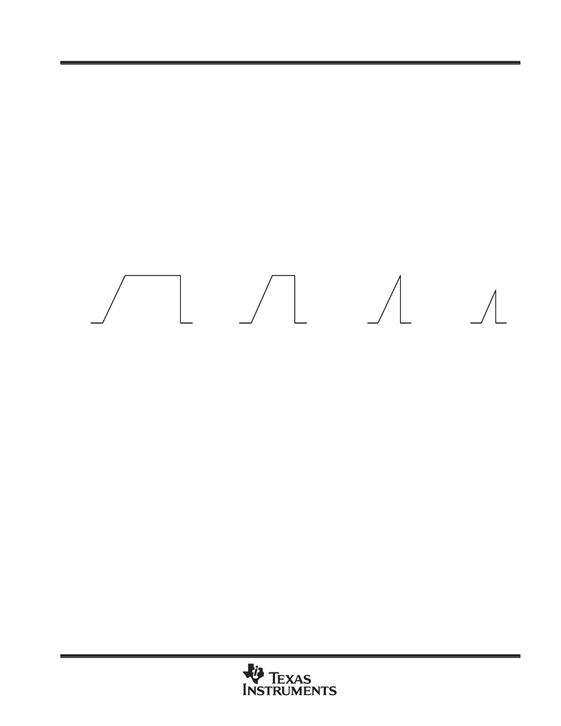
full-peak response is defined as the maximum output frequency, without regard to distortion, above which full
peak-to-peak output swing cannot be maintained.
Because there is no industry-wide accepted value for significant distortion, the full-peak response is specified
in this data sheet and is measured using the circuit of Figure 1. The initial setup involves the use of a sinusoidal
input to determine the maximum peak-to-peak output of the device (the amplitude of the sinusoidal wave is
increased until clipping occurs). The sinusoidal wave is then replaced with a square wave of the same
amplitude. The frequency is then increased until the maximum peak-to-peak output can no longer be maintained
(Figure 5). A square wave is used to allow a more accurate determination of the point at which the maximum
peak-to-peak output is reached.
(d) f > BOM
(c) f = BOM
(b) BOM > f > 100 kHz
(a) f = 100 kHz
Figure 5. Full-Power-Response Output Signal
test time
Inadequate test time is a frequent problem, especially when testing CMOS high-volume, short-test-time
environment. Internal capacitances are inherently higher in CMOS devices and require longer test times than
their bipolar and BiFET counterparts. The problem becomes more pronounced with reduced supply levels and
lower temperatures.
相關(guān)PDF資料 |
PDF描述 |
|---|---|
| 27L4000-20 | 4M-BIT [512K x8] LOW VOLTAGE OPERATION CMOS EPROM |
| 27L4000-25 | 4M-BIT [512K x8] LOW VOLTAGE OPERATION CMOS EPROM |
| 27L512-12 | 512K-BIT [64K x 8] CMOS EPROM |
| 27L512-15 | 512K-BIT [64K x 8] CMOS EPROM |
| 27L512-20 | 512K-BIT [64K x 8] CMOS EPROM |
相關(guān)代理商/技術(shù)參數(shù) |
參數(shù)描述 |
|---|---|
| 27L2C | 制造商:TI 制造商全稱:Texas Instruments 功能描述:LinCMOSE PRECISION DUAL OPERATIONAL AMPLIFIERS |
| 27L322 | 制造商:REGAL BELOIT 功能描述:OIL FILLED 制造商:Genteq 功能描述:OIL FILLED CAPACITOR |
| 27L327RR | 制造商:REGAL BELOIT 功能描述:OIL FILLED CAPACITOR |
| 27L33 | 制造商:Genteq 功能描述: |
| 27L33BX | 制造商:Genteq 功能描述: |
發(fā)布緊急采購(gòu),3分鐘左右您將得到回復(fù)。