- 您現(xiàn)在的位置:買賣IC網(wǎng) > PDF目錄371399 > 24LC65-ISM (Microchip Technology Inc.) 64K 2.5V I 2 C Smart Serial EEPROM PDF資料下載
參數(shù)資料
| 型號(hào): | 24LC65-ISM |
| 廠商: | Microchip Technology Inc. |
| 英文描述: | 64K 2.5V I 2 C Smart Serial EEPROM |
| 中文描述: | 64K的2.5VI 2葷智能串行EEPROM |
| 文件頁(yè)數(shù): | 8/12頁(yè) |
| 文件大小: | 106K |
| 代理商: | 24LC65-ISM |

24LC65
DS21073E-page 8
1996 Microchip Technology Inc.
5.7
Security Options
The 24LC65 has a sophisticated mechanism for
write-protecting portions of the array. This write protect
function is programmable and allows the user to protect
0-15 contiguous 4K blocks. The user sets the security
option by sending to the device the starting block num-
ber for the protected region and the number of blocks to
be protected. If the security option is invoked with 0
blocks protected, then all portions of the array will be
unprotected. All parts will come from the factory in the
default configuration with the starting block number set
to 15 and the number of protected blocks set to zero.
THE SECURITY OPTION CAN BE SET ONLY ONCE.
To invoke the security option, a write command is sent
to the device with the leading bit (bit 7) of the first
address byte set to a 1 (Figure 8-1). Bits 1-4 of the first
address byte define the starting block number for the
protected region. For example, if the starting block
number is to be set to 5, the first address byte would be
1XX0101X. Bits 0, 5 and 6 of the first address byte are
disregarded by the device and can be either high or low.
The device will acknowledge after the first address
byte. A byte of don’t care bits is then sent by the master,
with the device acknowledging afterwards. The third
byte sent to the device has bit 7 (S/HE) set high and bit
6 (R) set low. Bits 4 and 5 are don’t cares and bits 0-3
define the number of blocks to be write protected. For
example, if three blocks are to be protected, the third
byte would be 10XX0011. After the third byte is sent to
the device, it will acknowledge and a STOP bit is then
sent by the master to complete the command.
During a normal write sequence, if an attempt is made
to write to a protected address, no data will be written
and the device will not report an error or abort the com-
mand. If a write command is attempted across a
secure boundary, unprotected addresses will be written
and protected addresses will not.
5.8
Security Configuration Read
The status of the secure portion of memory can be read
by using the same technique as programming this
option except the READ bit (bit 6) of the configuration
byte is set to a one. After the configuration byte is sent,
the device will acknowledge and then send two bytes of
data to the master just as in a normal read sequence.
The master must acknowledge the first byte and not
acknowledge the second, and then send a stop bit to
end the sequence. The upper four bits of both of these
bytes will always be read as '1's. The lower four bits of
the first byte contains the starting secure block. The
lower four bits of the second byte contains the number
of secure blocks. The default starting secure block is fif-
teen and the default number of secure blocks is zero
6.0
ACKNOWLEDGE POLLING
Since the device will not acknowledge during a write
cycle, this can be used to determine when the cycle is
complete (this feature can be used to maximize bus
throughput). Once the stop condition for a write com-
mand has been issued from the master, the device ini-
tiates the internally timed write cycle. ACK polling can
be initiated immediately. This involves the master send-
ing a start condition followed by the control byte for a
write command (R/W = 0). If the device is still busy with
the write cycle, then no ACK will be returned. If the
cycle is complete, then the device will return the ACK
and the master can then proceed with the next read or
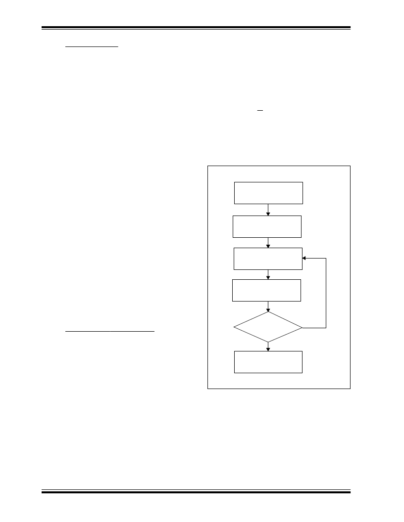
write command. See Figure 6-1 for flow diagram.
FIGURE 6-1:
ACKNOWLEDGE POLLING
FLOW
Send
Write Command
Send Stop
Condition to
Initiate Write Cycle
Send Start
Send Control Byte
with R/W = 0
Did Device
Acknowledge
(ACK = 0)
Next
Operation
NO
YES
相關(guān)PDF資料 |
PDF描述 |
|---|---|
| 24LC65-P | 64K 2.5V I 2 C Smart Serial EEPROM |
| 24LC65-SM | 64K 2.5V I 2 C Smart Serial EEPROM |
| 24LCS21A | 1K 2.5V Dual Mode I 2 C Serial EEPROM |
| 24LCS21 | 1K 2.5V Dual Mode I 2 C Serial EEPROM |
| 24LCS41A | 1K/4K 2.5V Dual Mode, Dual Port IIC Serial EEPROM(1K/4K位,2.5V雙模式,雙端口IIC串行EEPROM) |
相關(guān)代理商/技術(shù)參數(shù) |
參數(shù)描述 |
|---|---|
| 24LC65T/SM | 功能描述:電可擦除可編程只讀存儲(chǔ)器 8kx8 - 2.5V Smart RoHS:否 制造商:Atmel 存儲(chǔ)容量:2 Kbit 組織:256 B x 8 數(shù)據(jù)保留:100 yr 最大時(shí)鐘頻率:1000 KHz 最大工作電流:6 uA 工作電源電壓:1.7 V to 5.5 V 最大工作溫度:+ 85 C 安裝風(fēng)格:SMD/SMT 封裝 / 箱體:SOIC-8 |
| 24LC65T/SMG | 功能描述:電可擦除可編程只讀存儲(chǔ)器 8kx8 - 2.5V Smart Lead Free Package RoHS:否 制造商:Atmel 存儲(chǔ)容量:2 Kbit 組織:256 B x 8 數(shù)據(jù)保留:100 yr 最大時(shí)鐘頻率:1000 KHz 最大工作電流:6 uA 工作電源電壓:1.7 V to 5.5 V 最大工作溫度:+ 85 C 安裝風(fēng)格:SMD/SMT 封裝 / 箱體:SOIC-8 |
| 24LC65T-I/SM | 功能描述:電可擦除可編程只讀存儲(chǔ)器 8kx8 - 2.5V Smart RoHS:否 制造商:Atmel 存儲(chǔ)容量:2 Kbit 組織:256 B x 8 數(shù)據(jù)保留:100 yr 最大時(shí)鐘頻率:1000 KHz 最大工作電流:6 uA 工作電源電壓:1.7 V to 5.5 V 最大工作溫度:+ 85 C 安裝風(fēng)格:SMD/SMT 封裝 / 箱體:SOIC-8 |
| 24LC65T-I/SMG | 功能描述:電可擦除可編程只讀存儲(chǔ)器 8kx8 - 2.5V Smart Industrial Temp RoHS:否 制造商:Atmel 存儲(chǔ)容量:2 Kbit 組織:256 B x 8 數(shù)據(jù)保留:100 yr 最大時(shí)鐘頻率:1000 KHz 最大工作電流:6 uA 工作電源電壓:1.7 V to 5.5 V 最大工作溫度:+ 85 C 安裝風(fēng)格:SMD/SMT 封裝 / 箱體:SOIC-8 |
| 24LCS21A/P | 功能描述:電可擦除可編程只讀存儲(chǔ)器 2.5V Dual Mode RoHS:否 制造商:Atmel 存儲(chǔ)容量:2 Kbit 組織:256 B x 8 數(shù)據(jù)保留:100 yr 最大時(shí)鐘頻率:1000 KHz 最大工作電流:6 uA 工作電源電壓:1.7 V to 5.5 V 最大工作溫度:+ 85 C 安裝風(fēng)格:SMD/SMT 封裝 / 箱體:SOIC-8 |
發(fā)布緊急采購(gòu),3分鐘左右您將得到回復(fù)。