- 您現(xiàn)在的位置:買賣IC網(wǎng) > PDF目錄371396 > 24LC515 (Microchip Technology Inc.) 512K I2C CMOS Serial EEPROM PDF資料下載
參數(shù)資料
| 型號: | 24LC515 |
| 廠商: | Microchip Technology Inc. |
| 英文描述: | 512K I2C CMOS Serial EEPROM |
| 中文描述: | 為512k的I2C的CMOS串行EEPROM |
| 文件頁數(shù): | 6/22頁 |
| 文件大小: | 285K |
| 代理商: | 24LC515 |

24AA515/24LC515/24FC515
DS21673C-page 6
Preliminary
2003 Microchip Technology Inc.
4.0
BUS CHARACTERISTICS
The following
bus protocol
has been defined:
Data transfer may be initiated only when the bus
is not busy.
During data transfer, the data line must remain
stable whenever the clock line is high. Changes in
the data line while the clock line is high will be
interpreted as a Start or Stop condition.
Accordingly, the following bus conditions have been
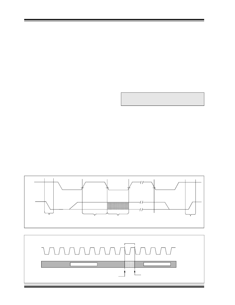
defined (Figure 4-1).
4.1
Bus not Busy (A)
Both data and clock lines remain high.
4.2
Start Data Transfer (B)
A high-to-low transition of the SDA line while the clock
(SCL) is high determines a Start condition. All
commands must be preceded by a Start condition.
4.3
Stop Data Transfer (C)
A low-to-high transition of the SDA line while the clock
(SCL) is high determines a Stop condition. All
operations must end with a Stop condition.
4.4
Data Valid (D)
The state of the data line represents valid data when,
after a Start condition, the data line is stable for the
duration of the high period of the clock signal.
The data on the line must be changed during the low
period of the clock signal. There is one bit of data per
clock pulse.
Each data transfer is initiated with a Start condition and
terminated with a Stop condition. The number of the
data bytes transferred between the Start and Stop
conditions is determined by the master device.
4.5
Acknowledge
Each receiving device, when addressed, is obliged to
generate an Acknowledge signal after the reception of
each byte. The master device must generate an extra
clock pulse which is associated with this Acknowledge
bit.
A device that acknowledges must pull-down the SDA
line during the Acknowledge clock pulse in such a way
that the SDA line is stable low during the high period of
the acknowledge related clock pulse. Of course, setup
and hold times must be taken into account. During
reads, a master must signal an end of data to the slave
by NOT generating an Acknowledge bit on the last byte
that has been clocked out of the slave. In this case, the
slave (24XX515) will leave the data line high to enable
the master to generate the Stop condition.
FIGURE 4-1:
DATA TRANSFER SEQUENCE ON THE SERIAL BUS
(D)
FIGURE 4-2:
ACKNOWLEDGE TIMING
Note:
The 24XX515 does not generate any
Acknowledge bits if an internal program-
ming cycle is in progress.
Address or
Acknowledge
Valid
Data
Allowed
To Change
Stop
Condition
Start
Condition
SCL
SDA
(A)
(B)
(D)
(C)
(A)
SCL
9
8
7
6
5
4
3
2
1
1
2
3
Transmitter must release the SDA line at this point
allowing the Receiver to pull the SDA line low to
acknowledge the previous eight bits of data.
Receiver must release the SDA line at this point
so the Transmitter can continue sending data.
Data from transmitter
Data from transmitter
SDA
Acknowledge
Bit
相關(guān)PDF資料 |
PDF描述 |
|---|---|
| 24FC65-IP | 64K 5.0V 1 MHz I 2 C Smart Serial EEPROM |
| 24FC65-ISM | 64K 5.0V 1 MHz I 2 C Smart Serial EEPROM |
| 24FC65-P | 64K 5.0V 1 MHz I 2 C Smart Serial EEPROM |
| 24FC65-SM | 64K 5.0V 1 MHz I 2 C Smart Serial EEPROM |
| 24FC65 | 64K 5.0V 1MHz CMOS Smart Serial EEPROMs(4.5~5.5V,64K位,10M次擦寫周期,IIC智能串行EEPROM) |
相關(guān)代理商/技術(shù)參數(shù) |
參數(shù)描述 |
|---|---|
| 24LC515-I/P | 功能描述:電可擦除可編程只讀存儲器 64kx8 64B - 2.5V RoHS:否 制造商:Atmel 存儲容量:2 Kbit 組織:256 B x 8 數(shù)據(jù)保留:100 yr 最大時鐘頻率:1000 KHz 最大工作電流:6 uA 工作電源電壓:1.7 V to 5.5 V 最大工作溫度:+ 85 C 安裝風(fēng)格:SMD/SMT 封裝 / 箱體:SOIC-8 |
| 24LC515-I/P | 制造商:Microchip Technology Inc 功能描述:IC EEPROM SERIAL 512K |
| 24LC515-I/SM | 功能描述:電可擦除可編程只讀存儲器 64kx8 64B - 2.5V RoHS:否 制造商:Atmel 存儲容量:2 Kbit 組織:256 B x 8 數(shù)據(jù)保留:100 yr 最大時鐘頻率:1000 KHz 最大工作電流:6 uA 工作電源電壓:1.7 V to 5.5 V 最大工作溫度:+ 85 C 安裝風(fēng)格:SMD/SMT 封裝 / 箱體:SOIC-8 |
| 24LC515-I/SM | 制造商:Microchip Technology Inc 功能描述:EEPROM SERIAL 512K 64B PAGE SMD |
| 24LC515ISM | 制造商:Microchip Technology Inc 功能描述: |
發(fā)布緊急采購,3分鐘左右您將得到回復(fù)。