- 您現(xiàn)在的位置:買賣IC網(wǎng) > PDF目錄368877 > 24C01SCS I2C Serial EEPROM PDF資料下載
參數(shù)資料
| 型號: | 24C01SCS |
| 英文描述: | I2C Serial EEPROM |
| 中文描述: | I2C串行EEPROM的 |
| 文件頁數(shù): | 3/12頁 |
| 文件大?。?/td> | 168K |
| 代理商: | 24C01SCS |
1999 Microchip Technology Inc.
DS21170D-page 3
24C01SC/02SC
TABLE 1-3:
AC CHARACTERISTICS
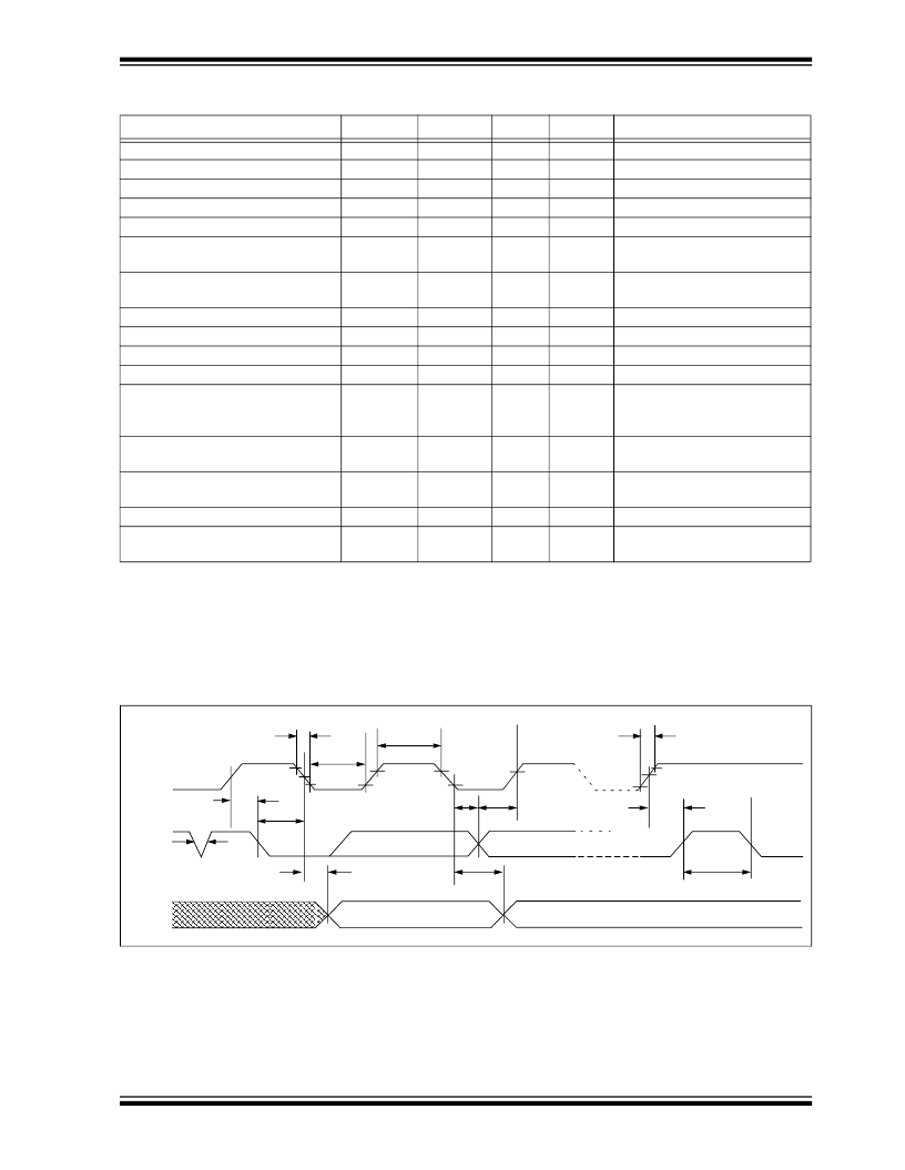
FIGURE 1-2:
BUS TIMING DATA
Parameter
Symbol
F
CLK
T
HIGH
T
LOW
T
R
T
F
T
HD
:
STA
Min.
—
600
1300
—
—
600
Max.
400
—
—
300
300
—
Units
kHz
ns
ns
ns
ns
ns
Remarks
Clock frequency
Clock high time
Clock low time
SDA and SCL rise time
SDA and SCL fall time
START condition hold time
(Note 1)
(Note 1)
After this period the first clock
pulse is generated
Only relevant for repeated
START condition
(Note 2)
START condition setup time
T
SU
:
STA
600
—
ns
Data input hold time
Data input setup time
STOP condition setup time
Output valid from clock
Bus free time
T
HD
:
DAT
T
SU
:
DAT
T
SU
:
STO
T
AA
T
BUF
0
—
—
—
900
—
ns
ns
ns
ns
ns
100
600
—
1300
(Note 2)
Time the bus must be free
before a new transmission can
start
(Note 1), CB e 100 pF
Output fall time from V
IH
minimum to V
IL
maximum
Input filter spike suppression
(SDA and SCL pins)
Write cycle time
Endurance
T
OF
20 +0.1
CB
—
250
ns
T
SP
50
ns
(Note 3)
T
WR
—
—
10
—
ms
Byte or Page mode
25°C, Vcc = 5V, Block Mode
(Note 4)
1M
cycles
Note 1: Not 100% tested. CB = total capacitance of one bus line in pF.
2: As a transmitter, the device must provide an internal minimum delay time to bridge the undefined region
(minimum 300 ns) of the falling edge of SCL to avoid unintended generation of START or STOP conditions.
3: The combined T
SP
and V
HYS
specifications are due to new Schmitt trigger inputs which provide improved
noise spike suppression. This eliminates the need for a TI specification for standard operation.
4: This parameter is not tested but guaranteed by characterization. For endurance estimates in a specific
application, please consult the Total Endurance Model which can be obtained on our website.
SCL
SDA
IN
SDA
OUT
T
HD
:
STA
T
SU
:
STA
T
F
T
HIGH
T
R
T
SU
:
STO
T
SU
:
DAT
T
HD
:
DAT
T
BUF
T
AA
T
HD
:
STA
T
AA
T
SP
T
LOW
This Material Copyrighted by Its Respective Manufacturer
相關(guān)PDF資料 |
PDF描述 |
|---|---|
| 24C01SCS08 | I2C Serial EEPROM |
| 24C01SCW | SCSI Terminator |
| 24C01SCW08 | SCSI Terminator |
| 24C01SCWF | I2C Serial EEPROM |
| 24C01SCWF08 | SCSI Terminator |
相關(guān)代理商/技術(shù)參數(shù) |
參數(shù)描述 |
|---|---|
| 24C01SC-S | 制造商:MICROCHIP 制造商全稱:Microchip Technology 功能描述:24C01C-P 24C01C-IP 24C01C-EP 24C01C-SN 24C01C-ISN 24C01C-ESN 24C01C-ST 24C01C-IST 24C01C-EST |
| 24C01SCS08 | 制造商:未知廠家 制造商全稱:未知廠家 功能描述:I2C Serial EEPROM |
| 24C01SC-S08 | 制造商:MICROCHIP 制造商全稱:Microchip Technology 功能描述:24C01C-P 24C01C-IP 24C01C-EP 24C01C-SN 24C01C-ISN 24C01C-ESN 24C01C-ST 24C01C-IST 24C01C-EST |
| 24C01SCW | 制造商:未知廠家 制造商全稱:未知廠家 功能描述:I2C Serial EEPROM |
| 24C01SC-W | 制造商:MICROCHIP 制造商全稱:Microchip Technology 功能描述:24C01C-P 24C01C-IP 24C01C-EP 24C01C-SN 24C01C-ISN 24C01C-ESN 24C01C-ST 24C01C-IST 24C01C-EST |
發(fā)布緊急采購,3分鐘左右您將得到回復(fù)。