- 您現(xiàn)在的位置:買賣IC網(wǎng) > PDF目錄371378 > 23710 Understanding Burst Mode Flash Memory Devices PDF資料下載
參數(shù)資料
| 型號: | 23710 |
| 英文描述: | Understanding Burst Mode Flash Memory Devices |
| 中文描述: | 理解突發(fā)模式閃存設備 |
| 文件頁數(shù): | 3/5頁 |
| 文件大小: | 78K |
| 代理商: | 23710 |

2
Understanding Burst Mode Flash Memory Devices
3…. Data is repeated if more than 32 clocks are sup-
plied.
All subsequent addresses are automatically generated
by the device at the rising edge of subsequent clock cy-
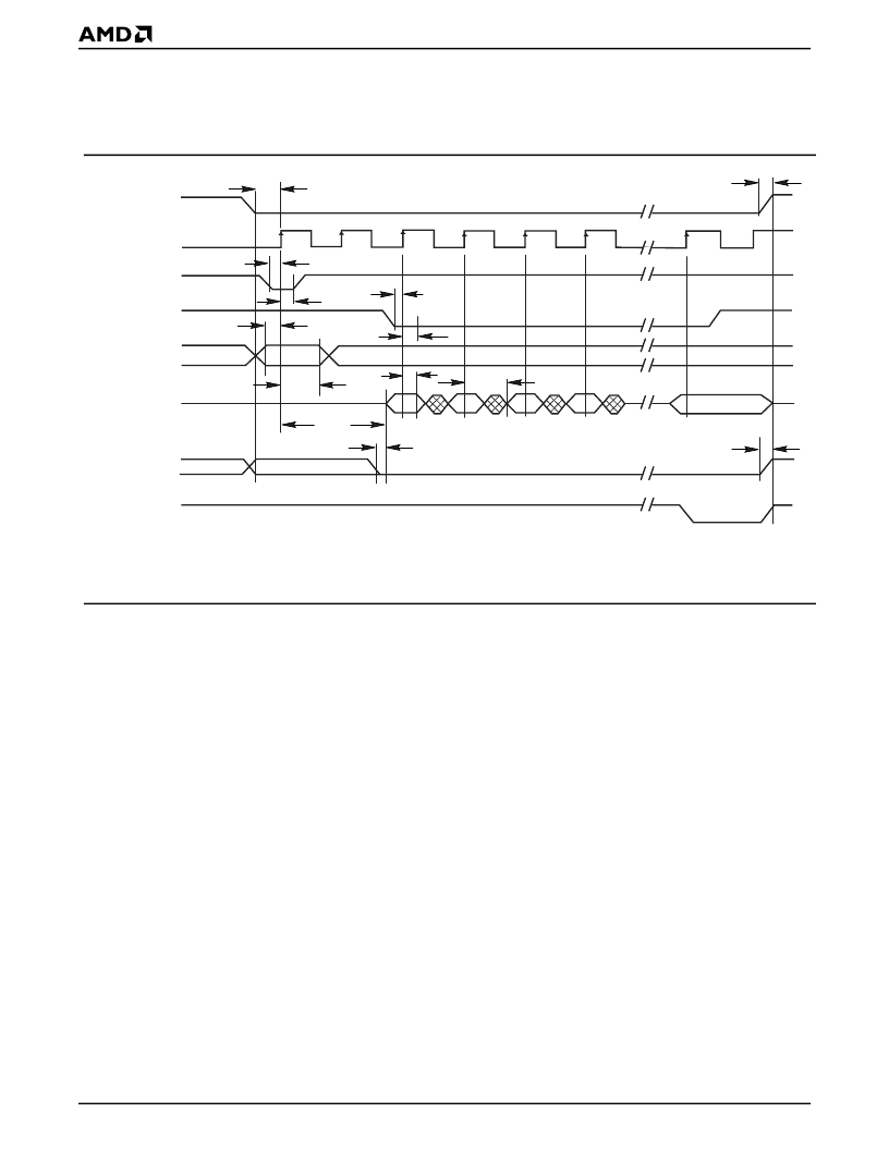
cles by the assertion of the BAA# signal. Figure 1
shows the timing diagram of a burst mode read opera-
tion.
Figure 1.
Timing Diagram For Burst Mode Read Operation
Note:
Timing diagram is based on the Am29BL162C datasheet. For more information on this device, refer to this document,
which is available at http://www.amd.com/products/nvd/ techdocs/22142.pdf.
In Figure 1, notice how the various signals must act to
achieve a burst mode read. After the first address (la-
beled “Aa”) is stabilized, the LBA# signal is driven low
at the first rising clock edge. This loads the first burst
address into the device. The LBA# signal is then driven
high and the address lines are “don’t care” for the re-
mainder of the burst mode read sequence.
After an access time of t
ACC
, the data from the first ad-
dress is available, and the device may now begin burst-
ing the data out. The address is incremented by driving
BAA# low (this is why the address lines are “don’t
care”). The data is now available t
BACC
after the previ-
ous read. At the end of the burst sequence, IND# goes
low to indicate that the data is the last data in the se-
quence.
Is There A Way To Suspend The Burst
Mode Operation
AMD burst mode devices are capable of Burst Sus-
pend and Burst Resume operations. The device enters
the Burst Suspend mode when BAA# is deasserted
(taken high). This means that the device will hold the
data that was being presented at the outputs when the
device was put into Burst Suspend operation. The pre-
sentation of data on the system data bus is indepen-
dently controlled by the OE# signal. The burst
operation can be resumed by asserting BAA#. Assert-
ing BAA# on the rising edge of the CLK will increment
the counter and present the next subsequent data at
the outputs after the specified t
BACC
time.
Terminating A Burst Mode Read
There are two ways to terminate a burst mode read op-
eration.
1.
Taking the RESET# pin low
will reset the device,
and it will default into reading array data in asyn-
chronous mode.
2.
Writing the Burst Disable command sequence
will
exit the device out of burst mode operation.
1.
Activating the LBA# (Low)
will terminate the previ-
ous burst read cycle and start a new burst read
cycle with the address that is currently valid.
Is The Burst Data Always Available T
BACC
After The Previous Read
While in burst mode operation, data will always be
available t
BACC
after the previous read. However, this
data may not always be read from the next address.
Recall that BAA# must be held low to increment the ad-
Da
Da + 2
Da + 3
Da + 31
OE#*
DQ0: DQ15
A0: A18
Aa
IND#
BAA#
LBA#
CLK
CE#
t
CES
t
BAAS
t
BAAH
t
ACS
t
LBAS
t
LBAH
t
ACH
t
OE
t
BACC
t
BDH
t
OEZ
t
CEZ
t
IACC
Da + 1
相關PDF資料 |
PDF描述 |
|---|---|
| 23711 | Understanding Page Mode Flash Memory Devices |
| 2375 | IEEE 802.3af PoE POWERED DEVICE CONTROLLERS WITH AUTO-RETRY |
| 2375-1 | IEEE 802.3af PoE POWERED DEVICE CONTROLLERS WITH AUTO-RETRY |
| 2376 | IEEE 802.3af PoE POWERED DEVICE CONTROLLERS WITH AUTO-RETRY |
| 2377 | IEEE 802.3af PoE POWERED DEVICE CONTROLLERS WITH AUTO-RETRY |
相關代理商/技術參數(shù) |
參數(shù)描述 |
|---|---|
| 237-100 | 制造商:RUKO 功能描述:DIE M10X1.5MM |
| 237-1001-000 | 制造商:ITT Interconnect Solutions 功能描述:C/N BACK-UP RING CV3459-10S / 237-1001-000 / Circular |
| 237-1002-000 | 制造商:ITT Interconnect Solutions 功能描述:CV3459-12&12S C/N RING / 237-1002-000 / Circular |
| 237-1003-000 | 制造商:ITT Interconnect Solutions 功能描述:CV3459-14&14S C/N RING / 237-1003-000 / Circular |
| 237-1004-000 | 制造商:ITT Interconnect Solutions 功能描述:CV3459-16&16 C/N RING / 237-1004-000 / Circular |
發(fā)布緊急采購,3分鐘左右您將得到回復。