- 您現(xiàn)在的位置:買賣IC網(wǎng) > PDF目錄368736 > 1725I (Linear Technology Corporation) General Purpose Isolated Flyback Controller PDF資料下載
參數(shù)資料
| 型號: | 1725I |
| 廠商: | Linear Technology Corporation |
| 英文描述: | General Purpose Isolated Flyback Controller |
| 中文描述: | 通用隔離反激式控制器 |
| 文件頁數(shù): | 10/28頁 |
| 文件大?。?/td> | 241K |
| 代理商: | 1725I |
第1頁第2頁第3頁第4頁第5頁第6頁第7頁第8頁第9頁當(dāng)前第10頁第11頁第12頁第13頁第14頁第15頁第16頁第17頁第18頁第19頁第20頁第21頁第22頁第23頁第24頁第25頁第26頁第27頁第28頁
10
LT1725
1725f
OPERATIOU
Enable Delay
When the output switch shuts off, the flyback pulse
appears. However, it takes a finite time until the trans-
former primary side voltage waveform approximately rep-
resents the output voltage. This is partly due to rise time
on the MOSFET drain node, but more importantly, due to
transformer leakage inductance. The latter causes a volt-
age spike on the primary side not directly related to output
voltage. (Some time is also required for internal settling of
the feedback amplifier circuitry.)
In order to maintain immunity to these phenomena, a
fixed delay is introduced between the switch turnoff
command and the enabling of the feedback amplifier. This
is termed “enable delay”. In certain cases where the
leakage spike is not sufficiently settled by the end of the
enable delay period, regulation error may result. See
Applications Information for further details.
Collapse Detect
Once the feedback amplifier is enabled, some mechanism
is then required to disable it. This is accomplished by a
collapse detect comparator, which compares the flyback
voltage (FB referred) to a fixed reference, nominally 80%
of V
BG
. When the flyback waveform drops below this
level, the feedback amplifier is disabled. This action
accommodates both continuous and discontinuous mode
operation.
Minimum Enable Time
The feedback amplifier, once enabled, stays enabled for a
fixed minimum time period termed “minimum enable
time.” This prevents lockup, especially when the output
voltage is abnormally low, e.g., during start-up. The mini-
mum enable time period ensures that the V
C
node is able
to “pump up” and increase the current mode trip point to
the level where the collapse detect system exhibits proper
operation. The “minimum enable time” often determines
the low load level at which output voltage regulation is lost.
See Applications Information for details.
Effects of Variable Enable Period
It should now be clear that the flyback amplifier is enabled
during only a portion of the cycle time. This can vary from
the fixed “minimum enable time” described to a maximum
of roughly the “off” switch time minus the enable delay
time. Certain parameters of flyback amp behavior will then
be directly affected by the variable enable period. These
include effective transconductance and V
C
node slew rate.
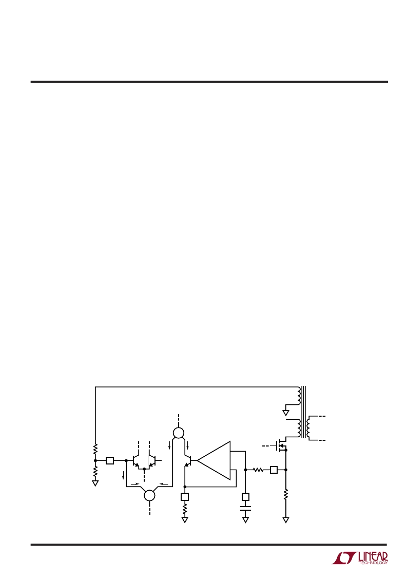
LOAD COMPENSATION THEORY
The LT1725 uses the flyback pulse to obtain information
about the isolated output voltage. A potential error source
is caused by transformer secondary current flow through
the real life nonzero impedances of the output rectifier,
T1
M1
R3
50k
V
IN
R2
LOAD
COMP I
R1
FB
V
BG
Q1 Q2
I
M
I
M
R
OCMP
R
CMPC
R
SENSE
I
SENSE
1725 F01
Q3
–
+
A1
Figure 1. Load Compensation Diagram
相關(guān)PDF資料 |
PDF描述 |
|---|---|
| 17537-5 | HTSNK B LONG .9H LOW FLOW, THRU HOLE |
| 17537 | HTSNK B LONG .9H LOW FLOW, THRU HOLE |
| 17539 | HTSNK, C LONG,. .911 LOW FLOW. THRU HOLE |
| 17539-G | SP Relay Socket |
| 17574 | HTSNK. C X-FLOW, .9H LOW FLOW. THRU HOLE |
相關(guān)代理商/技術(shù)參數(shù) |
參數(shù)描述 |
|---|---|
| 1725S-1C-12D | 制造商:Guardian Electric Manufacturing 功能描述: |
| 1725S-1C-24D | 制造商:Guardian Electric Manufacturing 功能描述: 制造商:M.E.C. Relays 功能描述: |
| 1726 | 功能描述:端子 ANVIL FOR TERMINALS RoHS:否 制造商:AVX 產(chǎn)品:Junction Box - Wire to Wire 系列:9826 線規(guī):26-18 接線柱/接頭大小: 絕緣: 顏色:Red 型式:Female 觸點(diǎn)電鍍:Tin over Nickel 觸點(diǎn)材料:Beryllium Copper, Phosphor Bronze 端接類型:Crimp |
| 1726 220 2101 | 制造商:Harting Technology Group 功能描述:SOCKET BUS TYPE 47 FEMALE R/A 220WAY |
| 1726 220 2102 | 制造商:Harting Technology Group 功能描述:SOCKET FEMALE R/A TYPE 47 220WAY 制造商:Harting Technology Group 功能描述:SOCKET, FEMALE, R/A, TYPE 47, 220WAY 制造商:Harting Technology Group 功能描述:SOCKET, FEMALE, R/A, TYPE 47, 220WAY; Series:Har-Bus; Gender:Receptacle; No. of Contacts:220; No. of Rows:5; Pitch Spacing:2mm; Connector Mounting:PCB; Contact Termination:Press Fit Right Angle; Contact Material:Copper; SVHC:No SVHC ;RoHS Compliant: Yes |
發(fā)布緊急采購,3分鐘左右您將得到回復(fù)。