- 您現(xiàn)在的位置:買賣IC網(wǎng) > PDF目錄152712 > 14REC0607 RF/MICROWAVE DOWN CONVERTER PDF資料下載
參數(shù)資料
| 型號(hào): | 14REC0607 |
| 元件分類: | 上/下變頻器 |
| 英文描述: | RF/MICROWAVE DOWN CONVERTER |
| 封裝: | DIE-10 |
| 文件頁數(shù): | 1/8頁 |
| 文件大?。?/td> | 173K |
| 代理商: | 14REC0607 |
Pre-production
14REC0607
December 2005 - Rev 30-Dec-05
Mimix Broadband, Inc., 10795 Rockley Rd., Houston, Texas 77099
Tel: 281.988.4600 Fax: 281.988.4615 mimixbroadband.com
Characteristic Data and Specifications are subject to change without notice.
2005 Mimix Broadband, Inc.
Export of this item may require appropriate export licensing from the U.S. Government. In purchasing these parts, U.S. Domestic customers accept
their obligation to be compliant with U.S. Export Laws.
Mimix Broadband
’
s 11.0-17.0 GHz GaAs MMIC receiver has a noise
figure of 2.2 dB and 20.0 dB image rejection across the band. This
device is a three stage LNA followed by an image reject resistive
pHEMT mixer and includes an integrated LO buffer amplifer. The image
reject mixer eliminates the need for a bandpass filter after the LNA to
remove thermal noise at the image frequency. I and Q mixer outputs
are provided and an external 90 degree hybrid is required to select the
desired sideband. This MMIC uses Mimix Broadband
’
s 0.15
m GaAs
PHEMT device model technology, and is based upon electron beam
lithography to ensure high repeatability and uniformity. The chip has
surface passivation to protect and provide a rugged part with backside
via holes and gold metallization to allow either a conductive epoxy or
eutectic solder die attach process. This device is well suited for
Millimeter-wave Point-to-Point Radio, LMDS, SATCOM and VSAT
applications.
11.0-17.0 GHz GaAs MMIC
Receiver
Page 1 of 8
Fully Integrated Design
2.2 dB Noise Figure
13.5 dB Conversion Gain
20 dB Image Rejection
+4 dBm IIP3
+3 dBm LO drive Level
100% On-Wafer RF, DC and Noise Figure Testing
100% Visual Inspection to MIL-STD-883 Method 2010
Features
General Description
Absolute Maximum Ratings
Supply Voltage (Vd)
Supply Current (Id1), (Id3)
Gate Bias Voltage (Vg)
Input Power (RF Pin)
Storage Temperature (Tstg)
Operating Temperature (Ta)
Channel Temperature (Tch)
+6.0 VDC
250, 200 mA
+0.3 VDC
+17 dBm
-65 to +165 OC
-55 to MTTF Table
MTTF Table
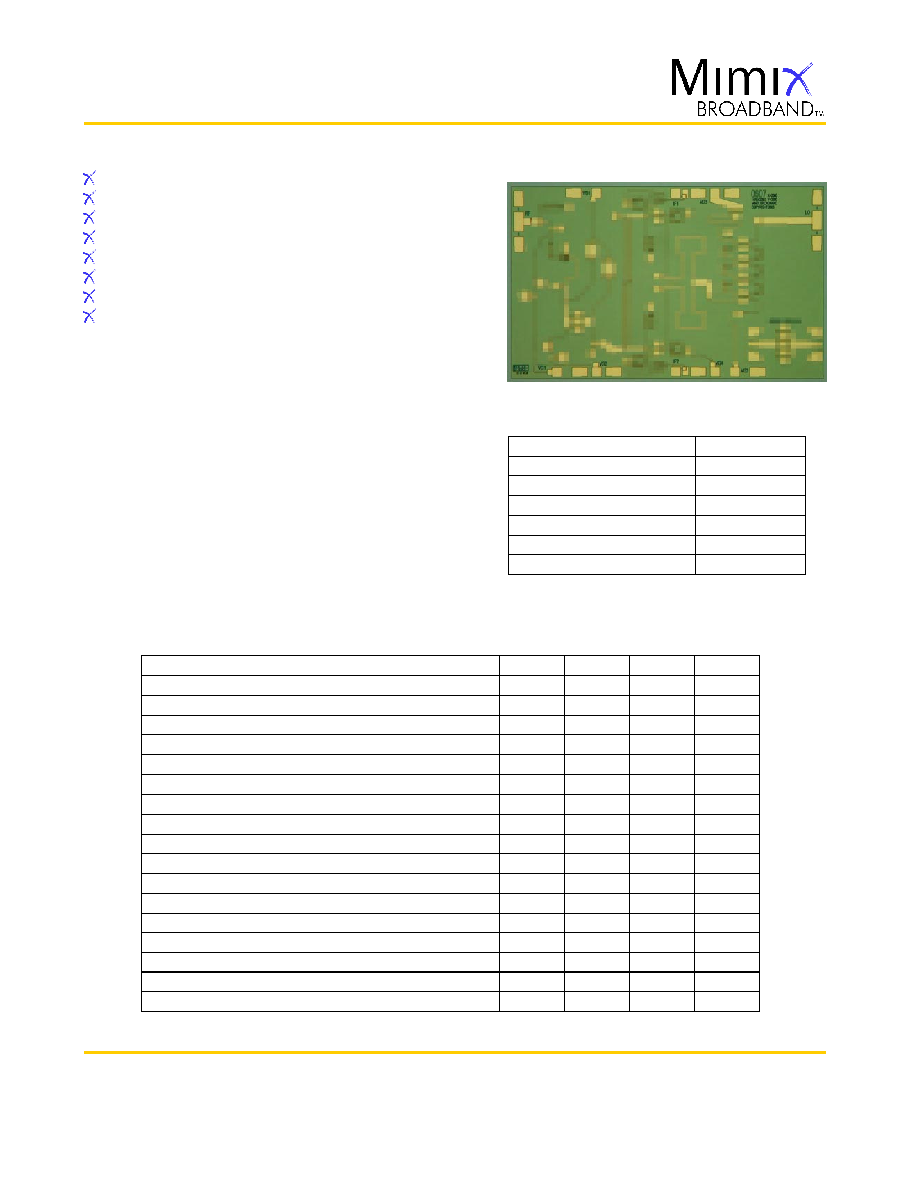
Chip Device Layout
(3) Channel temperature affects a device's MTTF. It is
recommended to keep channel temperature as low as
possible for maximum life.
3
Electrical Characteristics (AmbientTemperatureT = 25o C)
Units
GHz
dB
dBm
dBc
dB
dBm
VDC
mA
Min.
11.0
9.0
DC
-
-1.2
-
Typ.
-
2.0
15.0
13.5
+3.0
20.0
2.2
40.0/40.0
+4.0
+3.0
+5.0
-0.3
-0.1
-0.5
80
100
Max.
17.0
19.0
TBD
-
+6.0
+0.1
200
150
Parameter
Frequency Range (RF)
Frequency Range (LO)
Frequency Range (IF)
Input Return Loss RF (S11)
Small Signal Conversion Gain RF/IF (S21)
LO Input Drive (PLO)
Image Rejection
Noise Figure (NF)
Isolation LO/RF
Input Third Order Intercept (IIP3)
Drain Bias Voltage (Vd1)
Drain Bias Voltage (Vd3)
Gate Bias Voltage (Vg1,2)
Gate Bias Voltage (Vg3)
Gate Bias Voltage (Vg4) Mixer, Doubler
Supply Current (Id1) (Vd1=3.0, Vg=-0.3V Typical)
Supply Current (Id3) (Vd3=5.0V,Vg=-0.1V Typical)
(1) Measured using constant current.
1
相關(guān)PDF資料 |
PDF描述 |
|---|---|
| 14REC0607 | RF/MICROWAVE DOWN CONVERTER |
| 14T26-SZLB-350-0LC | INTERCONNECTION DEVICE |
| 15.0044-0 | INTERCONNECTION DEVICE |
| 15.0046-3 | INTERCONNECTION DEVICE |
| 15.0044-3 | INTERCONNECTION DEVICE |
相關(guān)代理商/技術(shù)參數(shù) |
參數(shù)描述 |
|---|---|
| 14RPLTRD | 制造商:Hammond Manufacturing 功能描述:closed bezel |
| 14RZD00001 | 制造商:MADISON CABLE / TE 功能描述: 制造商:Madison Cable / TE 功能描述: |
| 14S | 制造商:TE Connectivity 功能描述: |
| 14S10 | 功能描述:電氣外殼配件 TERMINAL BRACKET L8 RoHS:否 制造商:Hammond Manufacturing 產(chǎn)品:Rack Accessories 類型: 面板寬度: 面板高度: 外部寬度: 外部高度: 外部深度: 顏色:Black |
| 14S12 | 功能描述:電氣外殼配件 TERMINAL BRACKET L10 RoHS:否 制造商:Hammond Manufacturing 產(chǎn)品:Rack Accessories 類型: 面板寬度: 面板高度: 外部寬度: 外部高度: 外部深度: 顏色:Black |
發(fā)布緊急采購,3分鐘左右您將得到回復(fù)。