- 您現(xiàn)在的位置:買賣IC網(wǎng) > PDF目錄293740 > 1430G5C TRANSCEIVER, PDFO PDF資料下載
參數(shù)資料
| 型號: | 1430G5C |
| 元件分類: | 數(shù)字傳輸電路 |
| 英文描述: | TRANSCEIVER, PDFO |
| 文件頁數(shù): | 4/10頁 |
| 文件大小: | 288K |
| 代理商: | 1430G5C |
Lucent Technologies Inc.
3
Advance Data Sheet
NetLight 1430G5 Type SONET/SDH
January 2000
Long-Reach Transceivers with Clock Recovery
Transmitter
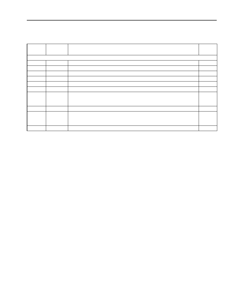
11
VCCT
Transmitter Power Supply.
NA
12
VEET
Transmitter Signal Ground.
NA
13
TDIS
Transmitter Disable.
LVTTL
14
TD+
Transmitter DATA In.
LVPECL
15
TD–
Transmitter DATA In Bar.
LVPECL
16
VEET
Transmitter Signal Ground.
NA
17
Bmon–
Laser Diode Bias Current Monitor—Negative End. The laser bias current
is accessible as a dc-voltage by measuring the voltage developed across pins
17 and 18.
NA
18
Bmon+
Laser Diode Bias Current Monitor—Positive End. See pin 17 description.
NA
19
Pmon–
Laser Diode Optical Power Monitor—Negative End. The back-facet diode
monitor current is accessible as a dc-voltage by measuring the voltage devel-
oped across pins 19 and 20.
NA
20
Pmon+
Laser Diode Optical Power Monitor—Positive End. See pin 19 description.
NA
Pin
Number
Symbol
Name/Description
Logic
Family
Electrostatic Discharge
Caution: This device is susceptible to damage as
a result of electrostatic discharge (ESD).
Take proper precautions during both
handling and testing. Follow
EIA* Stan-
dard EIA-625.
Although protection circuitry is designed into the
device, take proper precautions to avoid exposure to
ESD.
Lucent employs a human-body model (HBM) for ESD-
susceptibility testing and protection-design evaluation.
ESD voltage thresholds are dependent on the critical
parameters used to define the model. A standard HBM
(resistance = 1.5 k
, capacitance = 100 pF) is widely
used and, therefore, can be used for comparison pur-
poses. The HBM ESD threshold established for the
1430G5 transceiver is
±1000 V.
Application Information
The 1430 receiver section is a highly sensitive fiber-
optic receiver. Although the data outputs are digital
logic levels (PECL), the device should be thought of as
an analog component. When laying out system appli-
cation boards, the 1430 transceiver should receive the
same type of consideration one would give to a sensi-
tive analog component.
Printed-Wiring Board Layout Considerations
A fiber-optic receiver employs a very high gain, wide
bandwidth transimpedance amplifier. This amplifier
detects and amplifies signals that are only tens of nA in
amplitude when the receiver is operating near its sensi-
tivity limit. Any unwanted signal currents that couple
into the receiver circuitry cause a decrease in the
receiver's sensitivity and can also degrade the perfor-
mance of the receiver's signal detect (SD) circuit. To
minimize the coupling of unwanted noise into the
receiver, careful attention must be given to the printed-
wiring board.
At a minimum, a double-sided printed-wiring board
(PWB) with a large component-side ground plane
beneath the transceiver must be used. In applications
that include many other high-speed devices, a multi-
layer PWB is highly recommended. This permits the
placement of power and ground on separate layers,
which allows them to be isolated from the signal lines.
Multilayer construction also permits the routing of sen-
sitive signal traces away from high-level, high-speed
signal lines. To minimize the possibility of coupling
noise into the receiver section, high-level, high-speed
signals such as transmitter inputs and clock lines
should be routed as far away as possible from the
receiver pins.
*
EIA ia a registered tradenark of The Electronic Industries Associa
tion.
Pin Information (continued)
Table 1. Transceiver Pin Descriptions (continued)
相關(guān)PDF資料 |
PDF描述 |
|---|---|
| 1430G5C | TRANSCEIVER, PDFO |
| 1435096-1 | INTERCONNECTION DEVICE |
| 1437559-1 | TOGGLE SWITCH, DPDT, LATCHED, 4A, 28VDC, PANEL MOUNT-THREADED |
| 1449407-4 | INTERCONNECTION DEVICE |
| 1449411-8 | INTERCONNECTION DEVICE |
相關(guān)代理商/技術(shù)參數(shù) |
參數(shù)描述 |
|---|---|
| 1430G5LL | 制造商:AGERE 制造商全稱:AGERE 功能描述:NetLight 1430G5 Type SONET/SDH Long-Reach Transceivers with Clock Recovery |
| 14-30N | 制造商:Lighting Comp Design 功能描述:Intermediate Screw Grounded Or Non-Grounding Lamp Holder |
| 1430NF | 制造商:Platt Luggage 功能描述:1430 Top Loader Case (No foam) |
| 1431 | 制造商:PRO POWER (FORMERLY FROM SPC) 功能描述:TUBING SPLIT LOOM 12.523MM GREY 100F 制造商:PRO POWER (FORMERLY FROM SPC) 功能描述:TUBING, SPLIT LOOM, 12.523MM, GREY, 100F 制造商:VERNITRON - USE MOL 功能描述:Cross Referenced to MOLEX - Part: MOL38002-0185 制造商:pro-power 功能描述:TUBING, SPLIT LOOM, 12.523MM, GREY, 100FT; Sleeving / Tubing Type:Slit Loom; Length:30.5m; Sleeving Material:PE (Polyethylene); Internal Diameter:12.523mm; Sleeving Color:Grey; Leaded Process Compatible:No; Body Material:Polyethylene;RoHS Compliant: No |
| 14-31 | 功能描述:安裝硬件 Conn Cut-Out Cover ABS Black 94V-0 RoHS:否 制造商:Harwin 類型:SMT Cable Clip 材料:Phosphor Bronze 安裝孔大小: 長度:5 mm 外徑: 內(nèi)徑: 厚度: 電鍍:Tin 螺紋大小: |
發(fā)布緊急采購,3分鐘左右您將得到回復(fù)。