- 您現(xiàn)在的位置:買賣IC網(wǎng) > PDF目錄68779 > 12H2540-7 (POWER-ONE INC) 2-OUTPUT 50 W DC-DC REG PWR SUPPLY MODULE PDF資料下載
參數(shù)資料
| 型號: | 12H2540-7 |
| 廠商: | POWER-ONE INC |
| 元件分類: | 電源模塊 |
| 英文描述: | 2-OUTPUT 50 W DC-DC REG PWR SUPPLY MODULE |
| 封裝: | METAL, CASE H02, MODULE |
| 文件頁數(shù): | 7/19頁 |
| 文件大小: | 356K |
| 代理商: | 12H2540-7 |

Description of Options
Table 16: Survey of options
Option
Function of Option
Characteristic
-7
Extended operational ambient temperature range
TA = –25 to 71°C
D 1
Input and/or output undervoltage monitoring circuitry
Safe data signal output (D1 to D8)
V 1 2
Input and output undervoltage monitoring circuitry
ACFAIL signal according to VME specifications ( V2, V3)
1 Option D excludes option V and vice versa
2 Only available with main output voltage Vo1 = 5.1 V
-7 Extended Temperature Range
Option -7 extends the operational ambient temperature
range from –10 to 50 °C (standard) to –25 to 71 °C. The
power supplies provide full nominal output power with
convection cooling.
D Undervoltage Monitor
The input and/or output undervoltage monitoring circuit
operates independently of the built-in input undervoltage
lockout circuit. A logic "low" (JFET output) or "high" signal
(NPN output) is generated at pin 5 as soon as one of the
monitored voltages drops below the preselected threshold
level
Vt. The return for this signal is Vo1– (pin 23). The D
output recovers when the monitored voltage(s) exceed(s)
Vt+Vh. The threshold level Vt is adjustable by a
potentiometer, accessible through a hole in the front cover.
Option D exists in various versions D1 to D8 as shown in
the following table.
Table 17: Undervoltage monitor functions
Output type
Monitoring
Minimum adjustment range
Typical hysteresis
Vh [% of Vt]
JFET
NPN
Vi
Vo1
of threshold level
Vt
for Vt min to Vt max
Vti
Vto
Vhi
Vho
D1
D5
no
yes
–
3.5 V to 48 V 1
–
2.3 to 1
D2
D6
yes
no
Vi min to Vi max 1–
3.0 to 0.5
–
D3
D7
yes
Vi min to Vi max 1
0.95 to 0.98
Vo1 2
3.0 to 0.5
"0"
D4
D8
no
yes
–
0.95 to 0.98
Vo1 2
–
"0"
1 Threshold level adjustable by potentiometer (not recommended for mobile applications)
2 Fixed value between 95% and 98% of Vo1 (tracking)
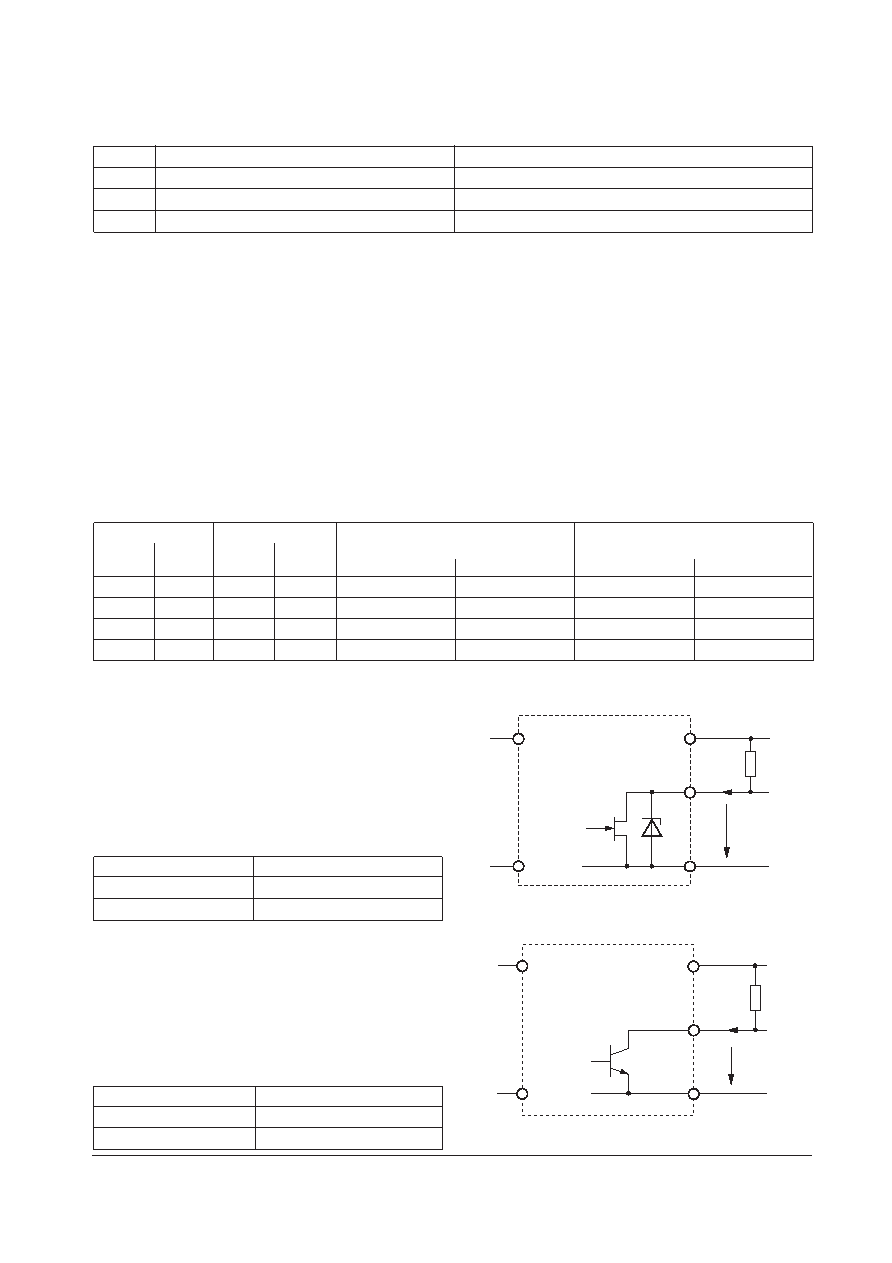
JFET output (D1 to D4):
Connector pin D is internally connected via the drain-
source path of a JFET (self-conducting type) to the
negative potential of output 1.
VD
≤ 0.4 V (logic low)
corresponds to a monitored voltage level (
Vi and/or Vo1)
<
Vt. The current ID through the JFET should not exceed 2.5
mA. The JFET is protected by a 0.5 W Zener diode of 8.2 V
against external overvoltages.
Vi, Vo1 status
D output,
VD
Vi or Vo1 < Vt
low, L,
VD
≤ 0.4 V at ID = 2.5 mA
Vi and Vo1 > Vt + Vh
high, H,
ID
≤ 25 A at VD = 5.25 V
Fig. 15
Options D1 to D4, JFET output
NPN output (D5 to D8):
Connector pin D is internally connected via the collector-
emitter path of an NPN transistor to the negative potential
of output 1.
VD - 0.4 V (logic low) corresponds to a
monitored voltage level (
Vi and/or Vo1) >Vt + Vh.The current
ID through the open collector should not exceed 20 mA. The
NPN output is not protected against external overvoltages.
VD should not exceed 40 V.
Vi, Vo1 status
D output,
VD
Vi or Vo1 < Vt
high, H,
ID
≤ 25 A at VD = 40 V
Vi and Vo1 > Vt +Vh
low, L,
VD
≤ 0.4 V at ID = 20 mA
Fig. 16
Options D5 to D8, NPN output
REV. MAR 27, 2006
Page 15 of 19
www.power-one.com
Vo1+
Vo1–
D
VD
ID
Rp
Input
11006
Vo1+
Vo1–
D
VD
ID
Rp
Input
11007
相關PDF資料 |
PDF描述 |
|---|---|
| 12H1901-2RD3 | 1-OUTPUT 50 W DC-DC REG PWR SUPPLY MODULE |
| 12H1901-2RD5 | 1-OUTPUT 50 W DC-DC REG PWR SUPPLY MODULE |
| 12H3020-2V3 | 3-OUTPUT 50 W DC-DC REG PWR SUPPLY MODULE |
| 12H3020-7D3 | 3-OUTPUT 50 W DC-DC REG PWR SUPPLY MODULE |
| 12H1001-7RD4 | 1-OUTPUT 50 W DC-DC REG PWR SUPPLY MODULE |
相關代理商/技術參數(shù) |
參數(shù)描述 |
|---|---|
| 12H28 | 制造商:未知廠家 制造商全稱:未知廠家 功能描述:Analog IC |
| 12H3 / 031158 | 制造商: 功能描述: 制造商:undefined 功能描述: |
| 12H3020-2 | 制造商:Power-One 功能描述: |
| 12H3040-2 | 制造商:Power-One 功能描述: |
| 12H4-50-0-1 | 制造商:HUBER+SUHNER 功能描述:RF COAXIAL CABLE MOUNT CONNECTOR |
發(fā)布緊急采購,3分鐘左右您將得到回復。