- 您現在的位置:買賣IC網 > PDF目錄40954 > YSS906N Stratix II GX FPGA 60K FPGA-1152 PDF資料下載
參數資料
| 型號: | YSS906N |
| 英文描述: | Stratix II GX FPGA 60K FPGA-1152 |
| 中文描述: | 消費性IC |
| 文件頁數: | 6/12頁 |
| 文件大?。?/td> | 0K |
| 代理商: | YSS906N |
YSS902
3
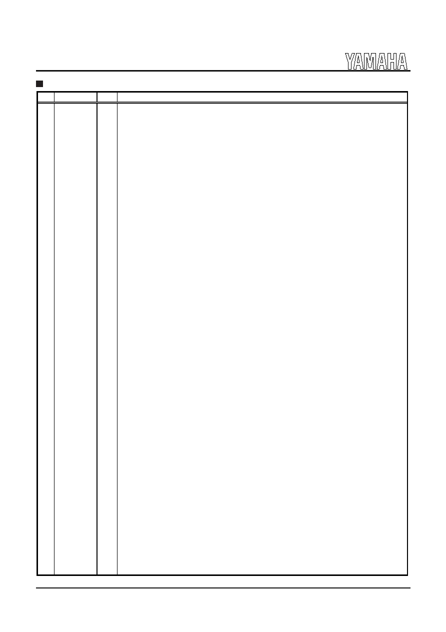
PIN FUNCTION
No.
Name
I/O
FUNCTION
1
VDD1
-
+5V power supply (for I/Os)
2
RAMCEN
O
External SRAM interface /CE
3
RAMA16
O
External SRAM interface address 16
4
RAMA15
O
External SRAM interface address 15
5SDIB0
I+
PCM input 0 to Sub DSP
6SDIB1
I+
PCM input 1 to Sub DSP
7SDIB2
I+
PCM input 2 to Sub DSP
8XI
I
Crystal oscillator connection (6.125MHz - 50.0MHz)
9XO
O
Crystal oscillator connection
10
VSS
-
Ground
11
AVDD
-
+3.3 V power supply (for PLL circuit)
12
TEST
Test terminal (to be open in normal use)
13
TEST
Test terminal (to be open in normal use)
14
TEST
Test terminal (to be open in normal use)
15
OVFB
O
Detection of overflow at Sub DSP
16
TEST
Test terminal (to be open in normal use)
17
TEST
Test terminal (to be open in normal use)
18
TEST
Test terminal (to be open in normal use)
19
CPO
A
Output terminal for PLL, to be connected to ground through the external analog filter circuit
20
AVSS
-
Ground (for PLL circuit)
21
VDD2
-
+3.3 V power supply (for core logic)
22
SDOA2
O
PCM output from Main DSP (C, LFE)
23
SDOA1
O
PCM output from Main DSP (LS, RS )
24
SDOA0
O
PCM output from Main DSP (L, R)
25
RAMA14
O
External SRAM interface address 14
26
RAMA13
O
External SRAM interface address 13
27
RAMA12
O
External SRAM interface address 12
28
RAMA11
O
External SRAM interface address 11
29
RAMA10
O
External SRAM interface address 10
30
VSS
-
Ground
31
VDD1
-
+5V power supply (for I/Os)
32
OPORT0
O
Output port for general purpose
33
OPORT1
O
Output port for general purpose
34
OPORT2
O
Output port for general purpose
35
OPORT3
O
Output port for general purpose
36
OPORT4
O
Output port for general purpose
37
OPORT5
O
Output port for general purpose
38
OPORT6
O
Output port for general purpose
39
OPORT7
O
Output port for general purpose
40
VSS
-
Ground
41
VDD2
-
+3.3 V power supply (for core logic)
42
RAMA9
O
External SRAM interface address 9
43
RAMA8
O
External SRAM interface address 8
44
RAMA7
O
External SRAM interface address 7
45
SDOB2
O
PCM output from Sub DSP
46
SDOB1
O
PCM output from Sub DSP
47
SDOB0
O
PCM output from Sub DSP
48
SDBCK1
I+
Bit clock input for SDOA, SDIB, SDOB
49
SDWCK1
I+
Word clock input for SDOA, SDIB, SDOB
50
VSS
-
Ground
51
VDD2
-
+3.3 V power supply (for core logic)
52
NONPCM
O
Detection of non-PCM data
53
CRC
O
Detection of CRC error
54
MUTE
O
Detection of auto mute
55
KARAOKE
O
Detection of AC-3 karaoke data
相關PDF資料 |
PDF描述 |
|---|---|
| YSS915-M | Stratix GX FPGA 40K 8-FBGA |
| YSS912F | Stratix GX FPGA 25K 16-FBGA |
| YST025J | 2.50mm PITCH CONNECTOR |
| YST025 | 2.50mm PITCH CONNECTOR |
| YST200-C | 2.00mm PITCH CONNECTOR |
相關代理商/技術參數 |
參數描述 |
|---|---|
| YSS912C | 制造商:未知廠家 制造商全稱:未知廠家 功能描述:DOLBY DIGITAL (AC-3) / PRO LOGIC / DTS DECODER + SUB DSP |
| YSS912F | 制造商:未知廠家 制造商全稱:未知廠家 功能描述:Consumer IC |
| YSS915 | 制造商:未知廠家 制造商全稱:未知廠家 功能描述:Karaoke Processor 2 for Video disc player |
| YSS915-M | 制造商:未知廠家 制造商全稱:未知廠家 功能描述:Consumer IC |
| YSS920B | 制造商:YAMAHA 制造商全稱:YAMAHA CORPORATION 功能描述:32位DSP引擎的各種聲音效果 |
發(fā)布緊急采購,3分鐘左右您將得到回復。