- 您現(xiàn)在的位置:買賣IC網(wǎng) > PDF目錄373749 > TWL2214CA High voltage fast-switching NPN power transistor PDF資料下載
參數(shù)資料
| 型號(hào): | TWL2214CA |
| 英文描述: | High voltage fast-switching NPN power transistor |
| 中文描述: | 電源管理IC和鋰離子電池充電控制 |
| 文件頁(yè)數(shù): | 22/36頁(yè) |
| 文件大小: | 511K |
| 代理商: | TWL2214CA |
第1頁(yè)第2頁(yè)第3頁(yè)第4頁(yè)第5頁(yè)第6頁(yè)第7頁(yè)第8頁(yè)第9頁(yè)第10頁(yè)第11頁(yè)第12頁(yè)第13頁(yè)第14頁(yè)第15頁(yè)第16頁(yè)第17頁(yè)第18頁(yè)第19頁(yè)第20頁(yè)第21頁(yè)當(dāng)前第22頁(yè)第23頁(yè)第24頁(yè)第25頁(yè)第26頁(yè)第27頁(yè)第28頁(yè)第29頁(yè)第30頁(yè)第31頁(yè)第32頁(yè)第33頁(yè)第34頁(yè)第35頁(yè)第36頁(yè)
/
/
S
–
–
T
–
1
–
9
2
P
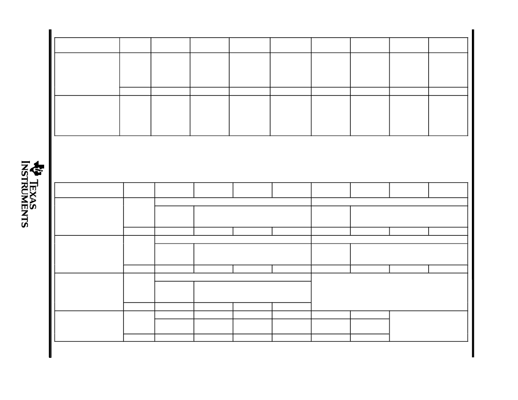
charger (continued)
REGISTER
ADDRESS
(HEX)
D7
(MSB)
D6
D5
D4
D3
D2
D1
D0
(LSB)
FCR1
: Function control
1Bh
(R/W)
CHGSTR
0 =
1 = Charger
Start
See Note 7
ADC status
0 = Disable
1 = Enable
See Notes 7
and 8
ADC function
0 = Single
1 = Periodically
See Notes 7
and 8
0
VBOT
1 = Battery
overvoltage
ADBV
0 = Disable
1 = Enable
See Notes 7
and 9
VTS
0 = Disable
1 = Enable
See Notes 7
and 10
ADCIN1
0 = Disable
1 = Enable
See Notes 7
and 10
ADCIN2
0 = Disable
1 = Enable
See Notes 7
and 10
IRQ
0 = IRQ is L
1 = IRQ is H
Default
0
0
0
0
0
0
0
SR:
STATUS register
1Ch
(R)
VEXT
1 = VCCHG in
range
BATERR
1 = Battery
error
CTERM
1 = Charge
current goes
below
termination out
NOCHG
1 = Charge
condition,
reset
CHGSTR to 0.
See Note 11
PCHG
1 = Precharge
mode
CCTO
1 = CC charge
timeout
TCTO
1 = Total
charge time
(CC+CV) out
NOTES:
7. After the TWL2214CA device has finished charging, these values are set to 0.
8. During CHGSTR H, ADC enables and periodically keeps functioning.
9. During charging mode ADVB is enabled automatically.
10. Charging mode is not necessary to set enable for function.
11. External microprocessor must set CHGSTR bit to 0 when NOCHG = 1
regulator, LED, VIBRATOR
REGISTER
ADDRESS
(HEX)
D7
(MSB)
D6
D5
D4
D3
D2
D1
D0
(LSB)
20h
(R/W)
REG2
REG3
FCR2:
Function register 2
0 = Disable
1 = Enable
000 = 3 V
111 = 2.3 V in 100-mV steps
0
REG4
000 = 3 V
101 = 2.5 V in 100-mV steps
0
REG6
000 = 3 V
101 = 2.5 V in 100-mV steps
0
Ringer
0 = Disable
1 = Enable
0
0 = Disable
1 = Enable
000 = 3 V
111 = 2.3 V in 100-mV steps
0
REG5
000 = 3 V
101 = 2.5 V in 100-mV steps
0
Default
0
0
0
0
0
0
FCR3:
Function register 3
21h
(R/W)
0 = Disable
1 = Enable
0 = Disable
1 = Enable
Default
0
0
0
0
0
0
FCR4:
Function register 4
22h
(R/W)
0 = Disable
1 = Enable
See Note 12
Don
’
t care
Default
0
0
0
23h
(R/W)
Vibrator
0 = Disable
1 = Enable
IL2
IL1
IL0
VG3_EN
0 = Disable
1 = Enable
0 See Note 13
FCR5:
Function register 5
0 = Disable
1 = Enable
0 = Disable
1 = Enable
0 = Disable
1 = Enable
Don
’
t care
Default
0
0
0
0
NOTES: 12. CONT = H, REG6 is dependent on D7 to enable. CONT = L, REG6 is independent of D7, always on after power up.
13. VG3_EN = 1, forces VG3 signal to Low. VG3_EN = 0, VG3 signal is at normal condition. Control of this bit is valid only when the adapter is connected.
相關(guān)PDF資料 |
PDF描述 |
|---|---|
| TX-1033S | TX-1033S |
| TX-S | SMALL POLARIZED RELAY WITH HIGH SENSITIVITY 50mW |
| TXC-20049-DCMM | N-channel 25V - 0.0068O - 60A - DPAK - IPAK STripFET™ III Power MOSFET |
| TXC-20153-DCMM | N-channel 30V - 0.0059 Ohm - 70A - DPAK / IPAK STripFET III Power MOSFET |
| TXC06303AIBG | N-CHANNEL 24V - 0.010 Ohm - 40A DPAK/IPAK ULTRA LOW GATE CHARGE STRIPFET POWER MOSFET |
相關(guān)代理商/技術(shù)參數(shù) |
參數(shù)描述 |
|---|---|
| TWL2214CAPFB | 制造商:Rochester Electronics LLC 功能描述:POWER SUPPLY MANAGEMENT IC:LION - Bulk 制造商:Texas Instruments 功能描述:CHGR LI-ION/LI-POL 150MA 2.8V 48TQFP - Tape and Reel |
| TWL2214CAPFBR | 制造商:Rochester Electronics LLC 功能描述:POWER SUPPLY MANAGEMENT IC:LION - Bulk 制造商:Texas Instruments 功能描述:CHGR LI-ION/LI-POL 150MA 2.8V 48TQFP - Tape and Reel |
| TWL2217CGGMR | 制造商:Texas Instruments 功能描述: |
| TWL2217CZQER | 制造商:Texas Instruments 功能描述: |
| TWL3014CGGMR | 制造商:Fairchild Semiconductor Corporation 功能描述: |
發(fā)布緊急采購(gòu),3分鐘左右您將得到回復(fù)。