- 您現(xiàn)在的位置:買賣IC網(wǎng) > PDF目錄299978 > TK63022BCB-G (TOKO INC) 2.2 V FIXED POSITIVE LDO REGULATOR, 0.262 V DROPOUT, PBGA4 PDF資料下載
參數(shù)資料
| 型號(hào): | TK63022BCB-G |
| 廠商: | TOKO INC |
| 元件分類: | 固定正電壓單路輸出LDO穩(wěn)壓器 |
| 英文描述: | 2.2 V FIXED POSITIVE LDO REGULATOR, 0.262 V DROPOUT, PBGA4 |
| 封裝: | FC-4 |
| 文件頁數(shù): | 18/29頁 |
| 文件大小: | 525K |
| 代理商: | TK63022BCB-G |
第1頁第2頁第3頁第4頁第5頁第6頁第7頁第8頁第9頁第10頁第11頁第12頁第13頁第14頁第15頁第16頁第17頁當(dāng)前第18頁第19頁第20頁第21頁第22頁第23頁第24頁第25頁第26頁第27頁第28頁第29頁
TK630xxB
GC3-J013
Page 25
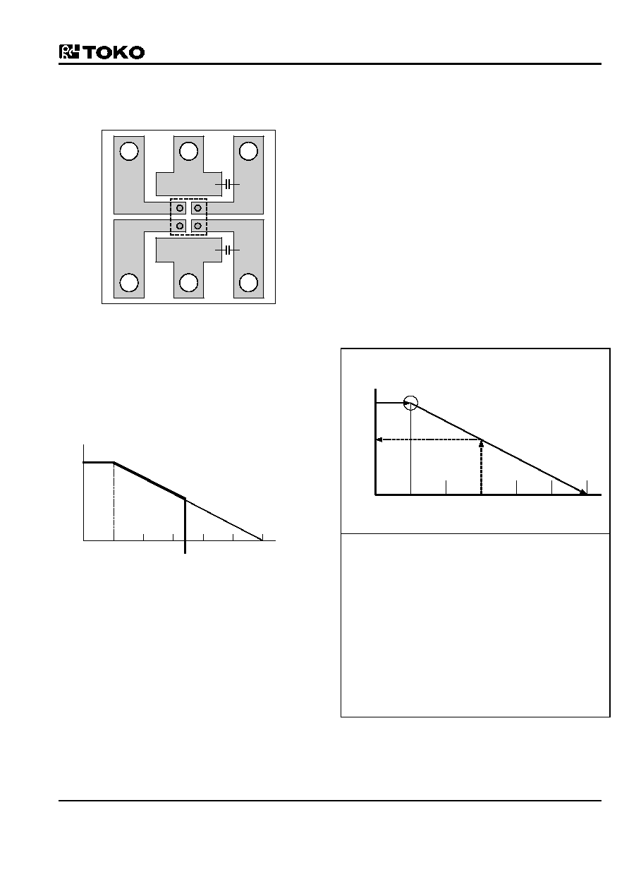
12-2. Layout
Fig12-4: Layout example
1
GND
V
Cont
V
In
V
Out
GND
(Top View)
PCB Material : Glass epoxy
Size : 7mm
×8mm×0.8mm
Please do derating with 2.9mW/
°C at Pd=360mW and
25
°C or more. Thermal resistance (θ
ja) is=278°C/W.
Fig12-5: Derating curve
25
50
100
150°C
Pd(mW)
360
(85°C)
-2.9mW/°C
The package loss is limited at the temperature that the
internal
temperature
sensor
works
(about
150
°C).
Therefore, the package loss is assumed to be an internal
limitation. There is no heat radiation characteristic of the
package unit assumed because of its small size. Heat is
carried away from the device by being mounted on the
PCB. This value is directly effected by the material and
the copper pattern etc. of the PCB. The losses are
approximately 360mW. Enduring these losses becomes
possible in a lot of applications operating at 25
°C.
The overheating protection circuit operates when the
junction temperature reaches 150
°C (this happens when
the regulator is dissipating excessive power, outside
temperature is high, or heat radiation is bad). The output
current and the output voltage will drop when the
protection circuit operates. However, operation begins
again as soon as the output voltage drops and the
temperature of the chip decreases.
How to determine the thermal resistance when
mounted on PCB
The thermal resistance when mounted is expressed as
follows:
T
j=θja×Pd+Ta
T
j of IC is set around 150°C. Pd is the value when the
thermal sensor is activated.
If the ambient temperature is 25
°C, then:
150=
θ
ja×Pd+25
θ
ja=125/Pd (°C /mW)
Pd is easily calculated.
A simple way to determine Pd is to calculate V
In×IIn
when the output side is shorted. Input current gradually
falls as output voltage rises after working thermal
shutdown. You should use the value when thermal
equilibrium is reached. In many cases, heat radiation is
good, and Pd is 360mW or more.
Fig12-6: How to determine DPd
0
255075
100
150
Pd(mW)
Pd
D Pd
2
3
5
4
Ta (℃)
Procedure (When mounted on PCB.)
1. Find Pd (V
In×IIn
when the output side is short-
circuited).
2. Plot Pd against 25
°C.
3. Connect Pd to the point corresponding to the 150
°C
with a straight line.
4. In design, take a vertical line from the maximum
operating temperature (e.g., 75
°C) to the derating
curve.
5. Read off the value of Pd against the point at which the
vertical line intersects the derating curve. This is taken
as the maximum power dissipation DPd.
6. DPd
÷ (V
In,MAXVOut)=IOut (at 75°C)
The maximum output current at the highest operating
temperature will be I
Out DPd ÷ (VIn,MAXVOut).
Please use the device at low temperature with better
radiation. The lower temperature provides better quality.
相關(guān)PDF資料 |
PDF描述 |
|---|---|
| TK63135SCL | 3.5 V FIXED POSITIVE LDO REGULATOR, 0.42 V DROPOUT, PDSO5 |
| TK70403MTR | 1.03 V FIXED POSITIVE REGULATOR, PDSO6 |
| TK71133NTR | 3.25 V FIXED POSITIVE REGULATOR, PBCY3 |
| TK71118N | 1.75 V FIXED POSITIVE REGULATOR, PBCY3 |
| TK71118NTR | 1.75 V FIXED POSITIVE REGULATOR, PBCY3 |
相關(guān)代理商/技術(shù)參數(shù) |
參數(shù)描述 |
|---|---|
| TK630STL | 制造商:TOKO 制造商全稱:TOKO, Inc 功能描述:CMOS LDO REGULATOR WITH HIGH ACTIVE CONTROL ADVANCED |
| TK633 | 制造商:未知廠家 制造商全稱:未知廠家 功能描述:Low TC Precision Radial-Lead Film Resistors |
| TK633STL | 制造商:TOKO 制造商全稱:TOKO, Inc 功能描述:CMOS LDO REGULATOR WITH HIGH ACTIVE CONTROL ADVANCED |
| TK633V | 制造商:未知廠家 制造商全稱:未知廠家 功能描述:Low TC Precision Radial-Lead Film Resistors |
| TK634 | 制造商:未知廠家 制造商全稱:未知廠家 功能描述:Low TC Precision Radial-Lead Film Resistors |
發(fā)布緊急采購,3分鐘左右您將得到回復(fù)。