- 您現(xiàn)在的位置:買(mǎi)賣(mài)IC網(wǎng) > PDF目錄299975 > TICP107MLPR (BOURNS INC) 1 A, 600 V, SCR PDF資料下載
參數(shù)資料
| 型號(hào): | TICP107MLPR |
| 廠商: | BOURNS INC |
| 元件分類: | 晶閘管 |
| 英文描述: | 1 A, 600 V, SCR |
| 封裝: | PLASTIC, TO-92, 3 PIN |
| 文件頁(yè)數(shù): | 1/2頁(yè) |
| 文件大小: | 101K |
| 代理商: | TICP107MLPR |
TICP107 SERIES
SILICON CONTROLLED RECTIFIERS
P RO D UCT
INFORMA TION
1
JANUARY 1999 - REVISED SEPTEMBER 2002
Specifications are subject to change without notice.
● 1 A Continuous On-State Current
● 15 A Surge-Current
● Glass Passivated Wafer
● 400 V to 600 V Off-State Voltage
● IGT 50 A min, 200 A max
● di/dt 100A/s
● Package Options
PACKAGE
PACKING
PART # SUFFIX
LP
Bulk
(None)
LP with fomed leads
Tape and Reel
R
absolute maximum ratings over operating junction temperature (unless otherwise noted)
NOTES: 1. These values apply when the gate-cathode resistance RGK = 1 k.
2. These values apply for continuous dc operation with resistive load.
3. This value applies for one 50 Hz half-sine-wave when the device is operating at (or below) the rated value of peak reverse volta ge
and on-state current. Surge may be repeated after the device has returned to original thermal equilibrium.
4. Rate of rise of on-state current after triggering with IG = 10mA, diG/dt = 1A/s.
RATING
SYMBOL
VALUE
UNIT
Repetitive peak off-state voltage (see Note 1)
TICP107D
TICP107M
VDRM
400
600
V
Repetitive peak reverse voltage
TICP107D
TICP107M
VRRM
400
600
V
Continuous on-state current at (or below) 25°C ambient temperature (see Note 2)
IT(RMS)
1
A
Surge on-state current at (or below) 25°C ambient temperature (see Note 3)
ITSM
15
A
Critical rate of rise of on-state current at 110°C (see Note 4)
di/dt
100
A/s
Peak positive gate current (pulse width
≤ 300 s)
IGM
0.2
A
Junction temperature range
TJ
-40 to +110
°C
Storage temperature range
Tstg
-40 to +125
°C
Lead temperature 3.2 mm from case for 10 seconds
TL
230
°C
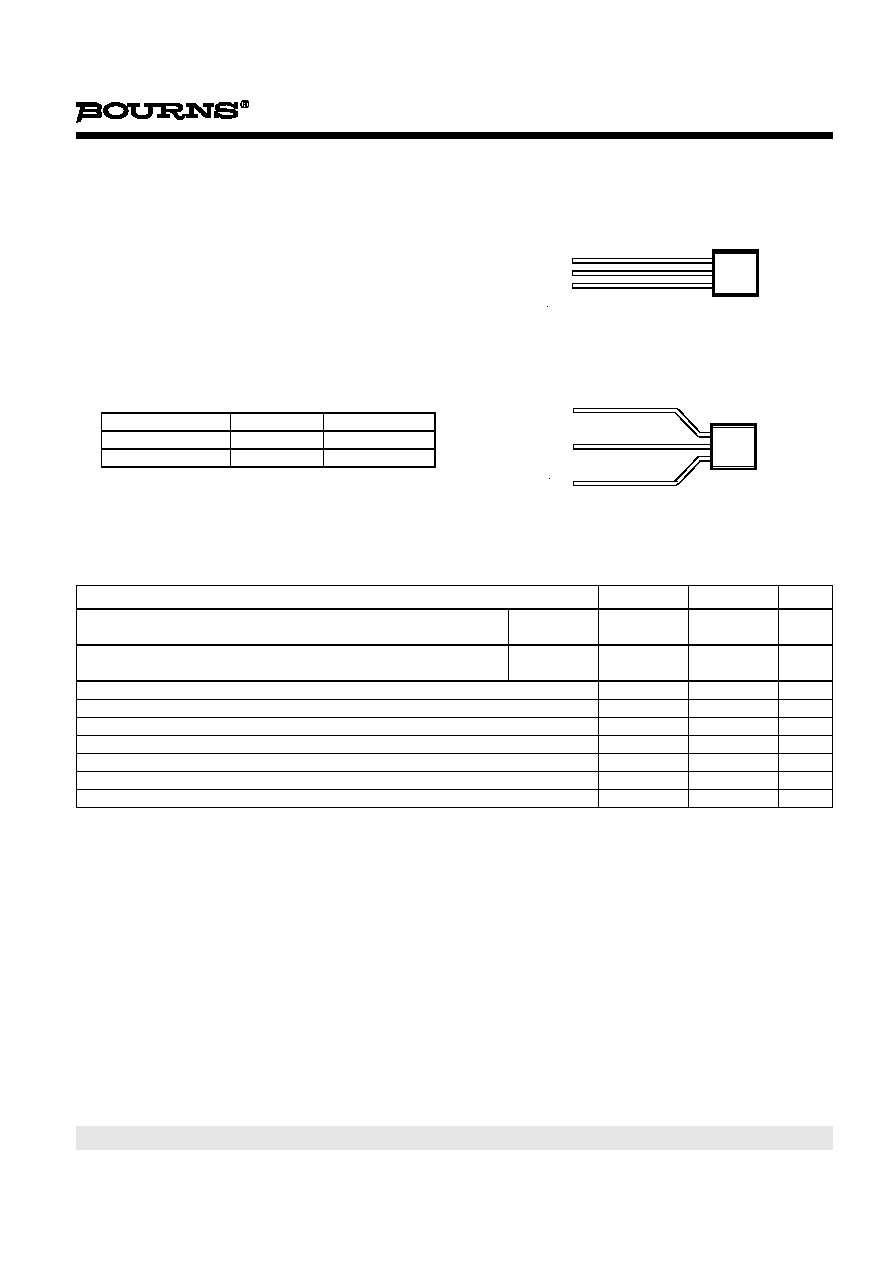
LP PACKAGE
(TOP VIEW)
MDC1AA
G
A
K
1
2
3
LP PACKAGE
WITH FORMED LEADS
(TOP VIEW)
MDC1AB
G
A
K
1
2
3
OBSOLET
E
相關(guān)PDF資料 |
PDF描述 |
|---|---|
| TICP107MLP | 1 A, 600 V, SCR, TO-92 |
| TIPC-36-5 | POWER TRANSFORMER, 5 VA |
| TIPC-36-56 | POWER TRANSFORMER, 56 VA |
| TIPC-36-30 | POWER TRANSFORMER, 30 VA |
| TIPC-36-20 | POWER TRANSFORMER, 20 VA |
相關(guān)代理商/技術(shù)參數(shù) |
參數(shù)描述 |
|---|---|
| TICP107MS | 制造商:Bourns Inc 功能描述: |
| TICP206 | 制造商:POINN 制造商全稱:Power Innovations Ltd 功能描述:SILICON TRIACS |
| TICP206D | 制造商:Bourns Inc 功能描述:TRIAC 1.5A 400V TO-92 |
| TICP206D | 制造商:Bourns Inc 功能描述:TRIAC 1.5A 400V TO-92 |
| TICP206D-R | 制造商:Bourns Inc 功能描述: |
發(fā)布緊急采購(gòu),3分鐘左右您將得到回復(fù)。