- 您現(xiàn)在的位置:買賣IC網(wǎng) > PDF目錄299957 > TC1017-2.6VCTTR 2.6 V FIXED POSITIVE LDO REGULATOR, 0.5 V DROPOUT, PDSO5 PDF資料下載
參數(shù)資料
| 型號: | TC1017-2.6VCTTR |
| 元件分類: | 固定正電壓單路輸出LDO穩(wěn)壓器 |
| 英文描述: | 2.6 V FIXED POSITIVE LDO REGULATOR, 0.5 V DROPOUT, PDSO5 |
| 封裝: | PLASTIC, MO-178, SOT-23, 5 PIN |
| 文件頁數(shù): | 4/22頁 |
| 文件大小: | 357K |
| 代理商: | TC1017-2.6VCTTR |
TC1017
DS21813D-page 12
2005 Microchip Technology Inc.
5.0
THERMAL CONSIDERATIONS
5.1
Thermal Shutdown
Integrated thermal protection circuitry shuts the
regulator off when the die temperature exceeds
approximately 160°C. The regulator remains off until
the die temperature drops to approximately 150°C.
5.2
Power Dissipation: SC-70
The TC1017 is available in the SC-70 package. The
thermal
resistance
for
the
SC-70
package
is
approximately 450°C/W when the copper area used in
the PCB layout is similar to the JEDEC J51-7 high ther-
mal conductivity standard or semi-G42-88 standard.
For applications with a larger or thicker copper area,
the thermal resistance can be lowered. See AN792, “A
Method to Determine How Much Power a SOT-23 Can
Dissipate in an Application”, DS00792, for a method to
determine the thermal resistance for a particular appli-
cation.
The TC1017 power dissipation capability is dependant
upon several variables: input voltage, output voltage,
load current, ambient temperature and maximum
junction temperature. The absolute maximum steady-
state junction temperature is rated at +125°C. The
power dissipation within the device is equal to:
EQUATION 5-1:
The VIN x IGND term is typically very small when
compared to the (VIN–VOUT) x ILOAD term, simplifying
the power dissipation within the LDO to be:
EQUATION 5-2:
To
determine
the
maximum
power
dissipation
capability, the following equation is used:
EQUATION 5-3:
Given the following example:
Find:
1.
Internal power dissipation:
2.
Maximum allowable ambient temperature:
3.
Maximum
allowable
power
dissipation
at
desired ambient:
In this example, the TC1017 dissipates approximately
158.5 mW and the junction temperature is raised 71°C
over the ambient. The absolute maximum power
dissipation is 155 mW when given a maximum ambient
temperature of 55°C.
Input voltage, output voltage or load current limits can
also be determined by substituting known values in the
power dissipation equations.
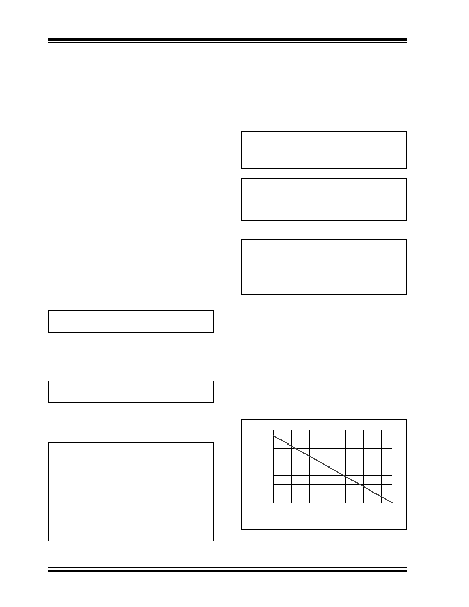
Figure 5-1 and Figure 5-2 depict typical maximum
power dissipation versus ambient temperature, as well
as typical maximum current versus ambient tempera-
ture, with a 1V input voltage to output voltage
differential, respectively.
FIGURE 5-1:
Power Dissipation vs.
Ambient Temperature (SC-70 package).
P
D
V
IN
V
OUT
–
() I
LOAD
V
IN
I
GN D
×
+
×
=
P
D
V
IN
V
OUT
–
() I
LOAD
×
=
P
DMAX
T
J_MAX
T
A_MAX
–
()
R
θ
JA
----------------------------------------------
=
Where:
TJ_MAX = the maximum junction
temperature allowed
TA_MAX = the maximum ambient
temperature
R
θJA
= the thermal resistance from
junction to air
VIN = 3.0V to 4.1V
VOUT = 2.85V ±2.5%
ILOAD = 120 mA (output current)
TA = 55°C (max. desired ambient)
P
DMAX
V
IN_MAX
V
OUT_MIN
–
() I
LOAD
×
=
4.1V
2.85
0.975
()
×
–
() 120mA
×
=
158.5mW
=
T
A_MAX
T
J_MAX
P
–
DM AX
R
θ
JA
×
=
125
°C 158.5mW 450°C/W
×
–
()
=
54
°C
=
125
°C71°C
–
()
=
P
D
T
J_MAX
T
A
–
R
θ
JA
------------------------------
=
155mW
=
125
°C55°C
–
450
°C/W
-----------------------------------
=
0
50
100
150
200
250
300
350
400
-40
-15
10
35
60
85
110
Ambient Temperature (°C)
P
o
w
e
rD
issi
pati
on
(m
W
)
相關(guān)PDF資料 |
PDF描述 |
|---|---|
| TC105550ECT | 5 V FIXED POSITIVE LDO REGULATOR, 0.25 V DROPOUT, PDSO5 |
| TC105550ECT723 | 5 V FIXED POSITIVE LDO REGULATOR, 0.25 V DROPOUT, PDSO5 |
| TC1301A-NICVMFTR | DUAL OUTPUT, FIXED POSITIVE LDO REGULATOR, PDSO8 |
| TC1301B-FFAVMFTR | DUAL OUTPUT, FIXED POSITIVE LDO REGULATOR, PDSO8 |
| TC1N5224B.TR | 2.8 V, 0.5 W, SILICON, UNIDIRECTIONAL VOLTAGE REGULATOR DIODE, DO-35 |
相關(guān)代理商/技術(shù)參數(shù) |
參數(shù)描述 |
|---|---|
| TC1017-3.0VCT | 制造商:MICROCHIP 制造商全稱:Microchip Technology 功能描述:150 mA, Tiny CMOS LDO With Shutdown |
| TC1017-3.0VCTTR | 功能描述:低壓差穩(wěn)壓器 - LDO 150mA CMOS LDO RoHS:否 制造商:Texas Instruments 最大輸入電壓:36 V 輸出電壓:1.4 V to 20.5 V 回動電壓(最大值):307 mV 輸出電流:1 A 負載調(diào)節(jié):0.3 % 輸出端數(shù)量: 輸出類型:Fixed 最大工作溫度:+ 125 C 安裝風格:SMD/SMT 封裝 / 箱體:VQFN-20 |
| TC1017-3.0VLT | 制造商:MICROCHIP 制造商全稱:Microchip Technology 功能描述:150 mA, Tiny CMOS LDO With Shutdown |
| TC1017-3.0VLTTR | 功能描述:低壓差穩(wěn)壓器 - LDO 150mA Adj LDO RoHS:否 制造商:Texas Instruments 最大輸入電壓:36 V 輸出電壓:1.4 V to 20.5 V 回動電壓(最大值):307 mV 輸出電流:1 A 負載調(diào)節(jié):0.3 % 輸出端數(shù)量: 輸出類型:Fixed 最大工作溫度:+ 125 C 安裝風格:SMD/SMT 封裝 / 箱體:VQFN-20 |
| TC1017-3.3VCT | 制造商:MICROCHIP 制造商全稱:Microchip Technology 功能描述:150 mA, Tiny CMOS LDO With Shutdown |
發(fā)布緊急采購,3分鐘左右您將得到回復。