- 您現(xiàn)在的位置:買賣IC網(wǎng) > PDF目錄299950 > T83C5101ZZZ-3ZSIL (ATMEL CORP) 8-BIT, MROM, 40 MHz, MICROCONTROLLER, PDIP24 PDF資料下載
參數(shù)資料
| 型號(hào): | T83C5101ZZZ-3ZSIL |
| 廠商: | ATMEL CORP |
| 元件分類: | 微控制器/微處理器 |
| 英文描述: | 8-BIT, MROM, 40 MHz, MICROCONTROLLER, PDIP24 |
| 封裝: | DIP-24 |
| 文件頁(yè)數(shù): | 45/52頁(yè) |
| 文件大小: | 701K |
| 代理商: | T83C5101ZZZ-3ZSIL |
第1頁(yè)第2頁(yè)第3頁(yè)第4頁(yè)第5頁(yè)第6頁(yè)第7頁(yè)第8頁(yè)第9頁(yè)第10頁(yè)第11頁(yè)第12頁(yè)第13頁(yè)第14頁(yè)第15頁(yè)第16頁(yè)第17頁(yè)第18頁(yè)第19頁(yè)第20頁(yè)第21頁(yè)第22頁(yè)第23頁(yè)第24頁(yè)第25頁(yè)第26頁(yè)第27頁(yè)第28頁(yè)第29頁(yè)第30頁(yè)第31頁(yè)第32頁(yè)第33頁(yè)第34頁(yè)第35頁(yè)第36頁(yè)第37頁(yè)第38頁(yè)第39頁(yè)第40頁(yè)第41頁(yè)第42頁(yè)第43頁(yè)第44頁(yè)當(dāng)前第45頁(yè)第46頁(yè)第47頁(yè)第48頁(yè)第49頁(yè)第50頁(yè)第51頁(yè)第52頁(yè)
Rev. F - 12 March, 2001
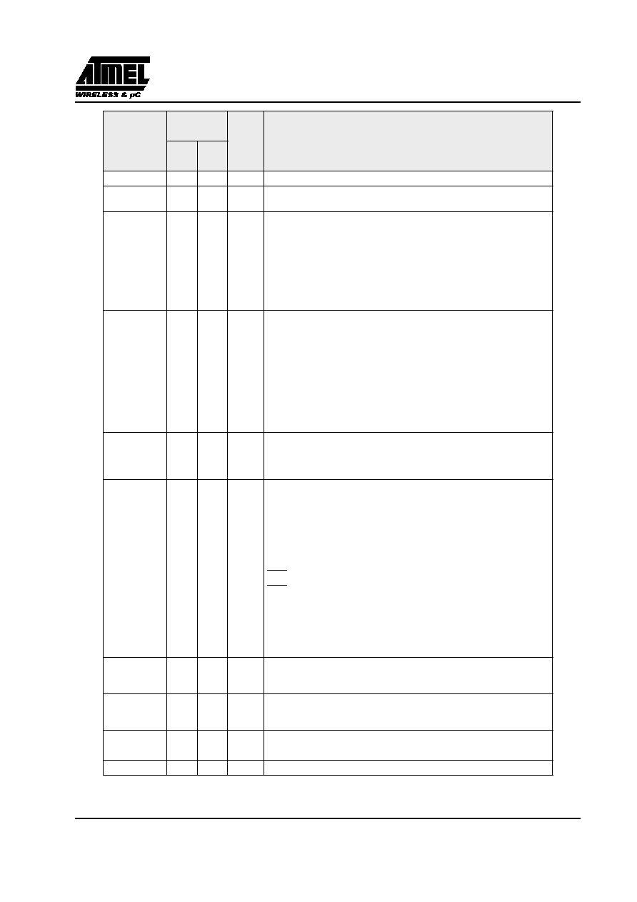
5
T87C5101
T83C5101/02
Mnemonic
Pin
Number
Type
Name and Function
24
pins
28
pins
VSS
12
14
I
Ground: 0V reference
VCC
24
28
I
Power Supply: This is the power supply voltage for normal, idle and power-
down operation
P1.0-P1.7
13-20
15-20
22-23
I/O
Port 1: Port 1 is an 8-bit bidirectional I/O port with internal pull-ups. Port 1 pins
that have 1s written to them are pulled high by the internal pull-ups and can be
used as inputs. As inputs, Port 1 pins that are externally pulled low will source
current because of the internal pull-ups. Port 1 also receives the low-order address
byte during memory programming and verification.
Alternate functions for Port 1 include:
I/O
T2 (P1.0): Timer/Counter 2 external count input/Clockout
I
T2EX (P1.1): Timer/Counter 2 Reload/Capture/Direction Control
P4.0
(Prog)-
P4.1 (Test)
7
8
9
O (I)
Port 4 bits 0 & 1: Except during programming and verifying, these two bits
are output port driving 30 micro Amps at high level and sinking 10 mA at low
level (Vol < 1V). If they have 1s written to them, they output a high level and
if they have 0 written to them, they output a low level. These 2 pins cannot be
used as inputs. Users should take care to never externally drive these pins
low, especially during reset. These two pins are primarily designed to drive
LEDs.
During programming and verifying, these two pins are used as input, as explained
in the corresponding chapter.
A Read or a Read/Modify/Write instruction to these bits will read the status of
the output: 1 if the output is 1, 0 if the output is 0.
P4.2-P4.5
NA
27
7
13
21
I/O
Port 4 bits 2 to 5: bidirectional I/O port with internal pull-ups. Port 4.2 to 4.5
pins that have 1s written to them are pulled high by the internal pull-ups and
can be used as inputs. As inputs, Port 4.2 to 4.5 pins that are externally pulled
low will source current because of the internal pull-ups.
P3.0-P3.7
5-1
23-21
5-1
26-24
I/O
Port 3: Port 3 is an 8-bit bidirectional I/O port with internal pull-ups. Port 3 pins
that have 1s written to them are pulled high by the internal pull-ups and can be
used as inputs. As inputs, Port 3 pins that are externally pulled low will source
current because of the internal pull-ups. Port 3 also serves the special features
of the 80C51 family, as listed below.
5
I
RxD (P3.0): Serial input port
4
O
TxD (P3.1): Serial output port
33
I
INT0 (P3.2): External interrupt 0
22
I
INT1 (P3.3): External interrupt 1
11
I
T0 (P3.4): Timer 0 external input
23
26
I
T1 (P3.5): Timer 1 external input
22
25
I/O
No alternate function on this pin
21
24
I/O
No alternate function on this pin
Reset
9
10
I
Reset: A high on this pin for two machine cycles while the oscillator is running,
resets the device. An internal diffused resistor to VSS permits a power-on reset
using only an external capacitor to VCC.
VPP
66
I
Programming Supply Voltage: This pin receives the 12.75V programming
supply voltage (VPP) during EPROM programming. During normal operation,
Vpp pin must be tied to Vcc.
XTAL1
11
12
I
Crystal 1: Input to the inverting oscillator amplifier and input to the internal
clock generator circuits.
XTAL2
10
11
O
Crystal 2: Output from the inverting oscillator amplifier
相關(guān)PDF資料 |
PDF描述 |
|---|---|
| T86N10BOF | 200 A, 1000 V, SCR |
| T930S20TOC | 2130 A, 2000 V, SCR |
| TA3-1W2K-V-T/R | KEYPAD SWITCH, SPST, MOMENTARY, 0.002A, 5VDC, 2.26 N, SURFACE MOUNT-RIGHT ANGLE |
| TA3-1R3-V-T/R | KEYPAD SWITCH, SPST, MOMENTARY, 0.002A, 5VDC, 3.04 N, SURFACE MOUNT-RIGHT ANGLE |
| TA3-2W2K-V-T/R | KEYPAD SWITCH, SPST, MOMENTARY, 0.002A, 5VDC, 2.26 N, SURFACE MOUNT-RIGHT ANGLE |
相關(guān)代理商/技術(shù)參數(shù) |
參數(shù)描述 |
|---|---|
| T83C5102 | 制造商:TEMIC 制造商全稱:TEMIC Semiconductors 功能描述:8-bit Low pin count Microcontrollers, 0-66 MHz |
| T83C5102XXX-3ZSCL | 制造商:ATMEL 制造商全稱:ATMEL Corporation 功能描述:8-bit Low Pin Count Microcontrollers |
| T83C5102XXX-3ZSCV | 制造商:ATMEL 制造商全稱:ATMEL Corporation 功能描述:8-bit Low Pin Count Microcontrollers |
| T83C5102XXX-3ZSIL | 制造商:ATMEL 制造商全稱:ATMEL Corporation 功能描述:8-bit Low Pin Count Microcontrollers |
| T83C5102XXX-ICFCL | 制造商:ATMEL 制造商全稱:ATMEL Corporation 功能描述:8-bit Low Pin Count Microcontrollers |
發(fā)布緊急采購(gòu),3分鐘左右您將得到回復(fù)。