- 您現(xiàn)在的位置:買賣IC網(wǎng) > PDF目錄299933 > ST24C04R (意法半導(dǎo)體) Serial 4K (512 x 8) EEPROM(串行4K EEPROM) PDF資料下載
參數(shù)資料
| 型號(hào): | ST24C04R |
| 廠商: | 意法半導(dǎo)體 |
| 英文描述: | Serial 4K (512 x 8) EEPROM(串行4K EEPROM) |
| 中文描述: | 串行4K的(512 × 8)的EEPROM(4K的串行EEPROM中) |
| 文件頁數(shù): | 16/16頁 |
| 文件大小: | 163K |
| 代理商: | ST24C04R |
ory address bits (A7-A3) are the same inside one
block. The master sends from one up to 8 bytes of
data, which are each acknowledged by the mem-
ory. After each byte is transfered, the internal byte
address counter (3 least significant bits only) is
incremented. The transfer is terminated by the
master generating a STOP condition. Care must be
taken to avoid address counter ’roll-over’ which
could result in data being overwritten. Note that, for
any write mode, the generation by the master of the
STOP condition starts the internal memory pro-
gram cycle. All inputs are disabled until the comple-
tion of this cycle and the memory will not respond
to any request.
Minimizing System Delays by Polling On ACK.
During the internal write cycle, the memory discon-
nects itself from the bus in order to copy the data
from the internal latches to the memory cells. The
maximum value of the write time (tW) is given in the
AC Characteristics table, since the typical time is
shorter, the time seen by the system may be re-
duced by an ACK polling sequence issued by the
master.
WRITE Cycle
in Progress
AI01099B
Next
Operation is
Addressing the
Memory
START Condition
DEVICE SELECT
with RW = 0
ACK
Returned
YES
NO
YES
NO
ReSTART
STOP
Proceed
WRITE Operation
Proceed
Random Address
READ Operation
Send
Byte Address
First byte of instruction
with RW = 0 already
decoded by ST24xxx
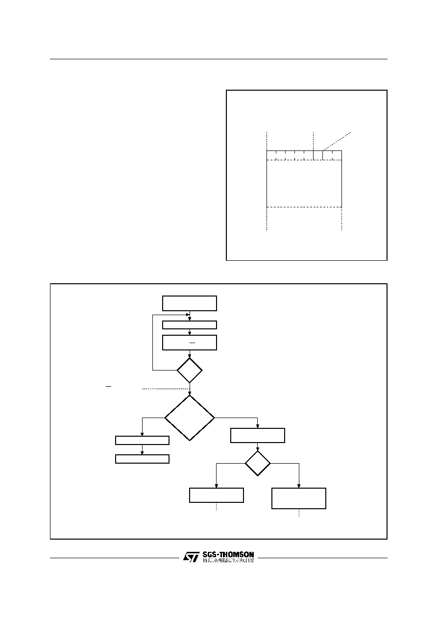
Figure 8. Write Cycle Polling using ACK
AI00855B
1FFh
b7
b3 b2
XX
100h
Block 1
Block 0
Protect Flag
Enable = 0
Disable = 1
8 byte
boundary
address
Protect Location
Figure 7. Memory Protection
9/16
ST24/25C04, ST24C04R, ST24/25W04
相關(guān)PDF資料 |
PDF描述 |
|---|---|
| ST25C08M1 | 1K X 8 SPI BUS SERIAL EEPROM, PDSO8 |
| ST280C04C1L | 960 A, 400 V, SCR, TO-200AB |
| ST280C04C2L | 960 A, 400 V, SCR, TO-200AB |
| ST280C04C2 | 960 A, 400 V, SCR, TO-200AB |
| ST280C04C3L | 960 A, 400 V, SCR, TO-200AB |
相關(guān)代理商/技術(shù)參數(shù) |
參數(shù)描述 |
|---|---|
| ST24C04RB1 | 制造商:未知廠家 制造商全稱:未知廠家 功能描述:I2C Serial EEPROM |
| ST24C04RB3 | 制造商:未知廠家 制造商全稱:未知廠家 功能描述:I2C Serial EEPROM |
| ST24C04RB5 | 制造商:未知廠家 制造商全稱:未知廠家 功能描述:I2C Serial EEPROM |
| ST24C04RB6 | 制造商:未知廠家 制造商全稱:未知廠家 功能描述:I2C Serial EEPROM |
| ST24C04RM1 | 制造商:未知廠家 制造商全稱:未知廠家 功能描述:I2C Serial EEPROM |
發(fā)布緊急采購(gòu),3分鐘左右您將得到回復(fù)。