- 您現(xiàn)在的位置:買賣IC網(wǎng) > PDF目錄193720 > SRM20V100SLBX7 128K X 8 STANDARD SRAM, 70 ns, PBGA32 PDF資料下載
參數(shù)資料
| 型號(hào): | SRM20V100SLBX7 |
| 元件分類: | SRAM |
| 英文描述: | 128K X 8 STANDARD SRAM, 70 ns, PBGA32 |
| 封裝: | PLASTIC, CSP-32 |
| 文件頁數(shù): | 6/10頁 |
| 文件大小: | 138K |
| 代理商: | SRM20V100SLBX7 |
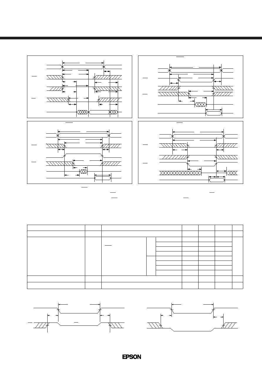
SRM20V100LLMX7/SLMX7
5
Note : 1. During read cycle time, WE is to be "H" level.
2. During write cycle time that is controlled by CS1 or CS2, Output Buffer is in high impedance state, whether OE level is "H" or "L".
3. During write cycle time that is controlled by WE, Output Buffer is high impedance state if OE is "H" level.
4. When I/O terminals are output mode, be careful that do not give the opposite signals to the I/O terminals.
rWrite Cycle (3) (WE Control)T3, T4
Address
CS1
CS2
WE
Dout
Din
tWC
tAW
tWP
tDW
tWR
tAS
tWHZ
tOW
DH
rWrite Cycle (2) (CS2 Control)T2
Address
CS1
CS2
WE
Dout
Din
tWC
tAW
tWP
tCW2
tCLZ2
tWHZ
tDW
tWR
tAS
tDH
rRead CylcleT1
Address
CS1
CS2
OE
Dout
rWrite Cycle (1) (CS1 Control)T2
Address
CS1
CS2
WE
Dout
Din
tWC
tAW
tCW1
tWHZ
tCLZ1
tDW
tWR
tAS
tDH
tOH
tCHZ1
tACS2
tCLZ2
tCHZ2
tOE
tOHZ
tOLZ
tRC
tACC
tACS1
tCLZ1
q Timing chart
T when retaining data in standby mode, supply voltage can be lowered with in a certain range. But read or write cycle
cannot be performed while the supply voltage is low.
q DATA RETENTION CHARACTERISTIC WITH LOW VOLTAGE POWER SUPPLY
Parameter
Symbol
Conditions
Min.
Typ.
Max.
Unit
Data retention Supply voltage
Data retention current
Chip select data hold time
VDDR
IDDR
tCDR
2.0
3.6
50
25
12
1.0
25
10
1.0
0.5
V
ns
(VSS = 0V, Ta = –25 to 85°C)
0
5
Operation recovery time
tR
ms
VDD = 3.0V
CS1 = CS2
≥VDD–0.2V
or CS2
≤0.2V
—
0.6
—
0.3
—
LL
SL
A
—
–25 to 85
°C
–25 to 70
°C
–25 to 40
°C
25
°C
–25 to 85
°C
–25 to 70
°C
–25 to 40
°C
25
°C
VDD
CS2
tCDR
tR
VIL
VDDR≥2.0V
CS2
≥0.2V
Data hold mode
Data retention timing
(CS1 Control)
3.0V
VDD
CS1
tCDR
VIH
tR
VIH
VDDR
≥2.0V
CS1
≥VDD—0.2V
Data hold mode
3.0V
Data retention timing
(CS2 Control)
相關(guān)PDF資料 |
PDF描述 |
|---|---|
| SRMMCC-3-R | QUARTZ CRYSTAL RESONATOR, 0.032768 MHz |
| SRMMCC-1-R | QUARTZ CRYSTAL RESONATOR, 0.032768 MHz |
| SRMMCC-2-R | QUARTZ CRYSTAL RESONATOR, 0.032768 MHz |
| SRMP49-24.0M | QUARTZ CRYSTAL RESONATOR, 24 MHz |
| SRN5124 | 20 MHz - 200 MHz RF/MICROWAVE WIDE BAND LOW POWER AMPLIFIER |
相關(guān)代理商/技術(shù)參數(shù) |
參數(shù)描述 |
|---|---|
| SRM20V100SLKX7 | 制造商:未知廠家 制造商全稱:未知廠家 功能描述:x8 SRAM |
| SRM20V100SLMX7 | 制造商:未知廠家 制造商全稱:未知廠家 功能描述:x8 SRAM |
| SRM20V100SLRX7 | 制造商:未知廠家 制造商全稱:未知廠家 功能描述:x8 SRAM |
| SRM20V100SLTX7 | 制造商:未知廠家 制造商全稱:未知廠家 功能描述:x8 SRAM |
| SRM20V100SLYX7 | 制造商:未知廠家 制造商全稱:未知廠家 功能描述:x8 SRAM |
發(fā)布緊急采購(gòu),3分鐘左右您將得到回復(fù)。