- 您現(xiàn)在的位置:買賣IC網(wǎng) > PDF目錄38624 > EQDP-056-33.00-TTR-STL-2-S (SAMTEC INC) INTERCONNECTION DEVICE PDF資料下載
參數(shù)資料
| 型號(hào): | EQDP-056-33.00-TTR-STL-2-S |
| 廠商: | SAMTEC INC |
| 元件分類: | 連接器件 |
| 英文描述: | INTERCONNECTION DEVICE |
| 文件頁數(shù): | 6/6頁 |
| 文件大小: | 4713K |
| 代理商: | EQDP-056-33.00-TTR-STL-2-S |
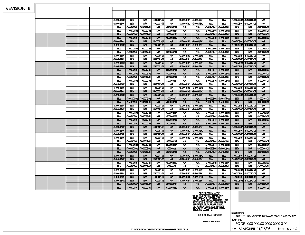
-TTR
-TTL
-TBR
-TBL
-STR
-STL
-SBR
-SBL
-TEU
-TED
-SEU
-SED
1
B14
2
1
2
B14
3
1
N-1
B14
4
1
N
B14
1
T1
2
1
2
T1
3
1
N-1
T1
4
1
N
T1
1
T1
2
1
2
T1
3
1
N-1
T1
4
1
N
T1
1
B14
2
1
2
B14
3
1
N-1
B14
4
1
N
B14
1
B1
2
1
2
B1
3
1
N-1
B1
4
1
N
B1
1
T14
2
1
2
T14
3
1
N-1
T14
4
1
N
T14
1
T14
2
1
2
T14
3
1
N-1
T14
4
1
N
T14
1
B1
2
1
2
B1
3
1
N-1
B1
4
1
N
B1
1
B14
2
1
2
B14
3
1
N-1
B14
4
1
N
B14
1
T1
2
1
2
T1
3
1
N-1
T1
4
1
N
T1
1
B1
2
1
2
B1
3
1
N-1
B1
4
1
N
B1
1
T14
2
1
2
T14
3
1
N-1
T14
4
1
N
T14
-TEU
-TED
-SEU
-SED
-T-XXX-03-01
-S-XXX-03-01
-STR
-STL
-SBR
-SBL
-TTR
-TTL
-TBR
-TBL
-S-XXX-01-01
-S-XXX-02-01
-S-XXX-01-01
-S-XXX-02-01
-T-XXX-01-01
-T-XXX-02-01
-T-XXX-01-01
-T-XXX-02-01
WIRE
#
FIRST END
SUB-EQCD-
X-XXX-XX-01
TABLE 9
SECOND END OPTION (SUB-EQCD-X-XXX-XX-XX)
FIRST
END
OPTION
WIRING
OPTION
FIRST
END
PIN #
SECOND
END
PIN #
S A MTEC
520 PARK EAST BLVD, NEW ALBANY, IN 47150
PHONE: 812.944.6733
FAX: 812.948.5047
e-Mail: INFO@SAMTEC.COM
CODE: 55322
相關(guān)PDF資料 |
PDF描述 |
|---|---|
| EQDP-056-33.00-TTR-STL-2-B | INTERCONNECTION DEVICE |
| EQDP-056-33.00-TTR-STL-1 | INTERCONNECTION DEVICE |
| EQDP-056-33.00-TTR-SEU-2-S | INTERCONNECTION DEVICE |
| EQDP-056-33.00-TTR-SEU-2-B | INTERCONNECTION DEVICE |
| EQDP-056-33.00-TTR-SEU-1-F | INTERCONNECTION DEVICE |
相關(guān)代理商/技術(shù)參數(shù) |
參數(shù)描述 |
|---|---|
| EQ-EPSILON-5 MK II | 制造商:Equinox Technologies 功能描述:UNIV. IN-SYSTEM PROG ((NS)) |
| EQF-17 | 制造商:Curtis Industries 功能描述: |
| EQ-F3-213 | 制造商:BRKLYN 功能描述: |
| EQF-5 | 制造商:Curtis Industries 功能描述: |
| EQF-8 | 制造商:Curtis Industries 功能描述: |
發(fā)布緊急采購,3分鐘左右您將得到回復(fù)。