- 您現(xiàn)在的位置:買賣IC網(wǎng) > PDF目錄299877 > S29GL128P10TFIR10 (SPANSION LLC) 3.0 Volt-only Page Mode Flash Memory featuring 90 nm MirrorBit Process Technology PDF資料下載
參數(shù)資料
| 型號(hào): | S29GL128P10TFIR10 |
| 廠商: | SPANSION LLC |
| 元件分類: | PROM |
| 英文描述: | 3.0 Volt-only Page Mode Flash Memory featuring 90 nm MirrorBit Process Technology |
| 中文描述: | 128M X 1 FLASH 3V PROM, 100 ns, PDSO56 |
| 封裝: | 20 X 14 MM, LEAD FREE, MO-142EC, TSOP-56 |
| 文件頁數(shù): | 69/80頁 |
| 文件大小: | 2706K |
| 代理商: | S29GL128P10TFIR10 |
第1頁第2頁第3頁第4頁第5頁第6頁第7頁第8頁第9頁第10頁第11頁第12頁第13頁第14頁第15頁第16頁第17頁第18頁第19頁第20頁第21頁第22頁第23頁第24頁第25頁第26頁第27頁第28頁第29頁第30頁第31頁第32頁第33頁第34頁第35頁第36頁第37頁第38頁第39頁第40頁第41頁第42頁第43頁第44頁第45頁第46頁第47頁第48頁第49頁第50頁第51頁第52頁第53頁第54頁第55頁第56頁第57頁第58頁第59頁第60頁第61頁第62頁第63頁第64頁第65頁第66頁第67頁第68頁當(dāng)前第69頁第70頁第71頁第72頁第73頁第74頁第75頁第76頁第77頁第78頁第79頁第80頁
November 20, 2009 S29GL-P_00_A12
S29GL-P MirrorBit Flash Family
71
Data
She e t
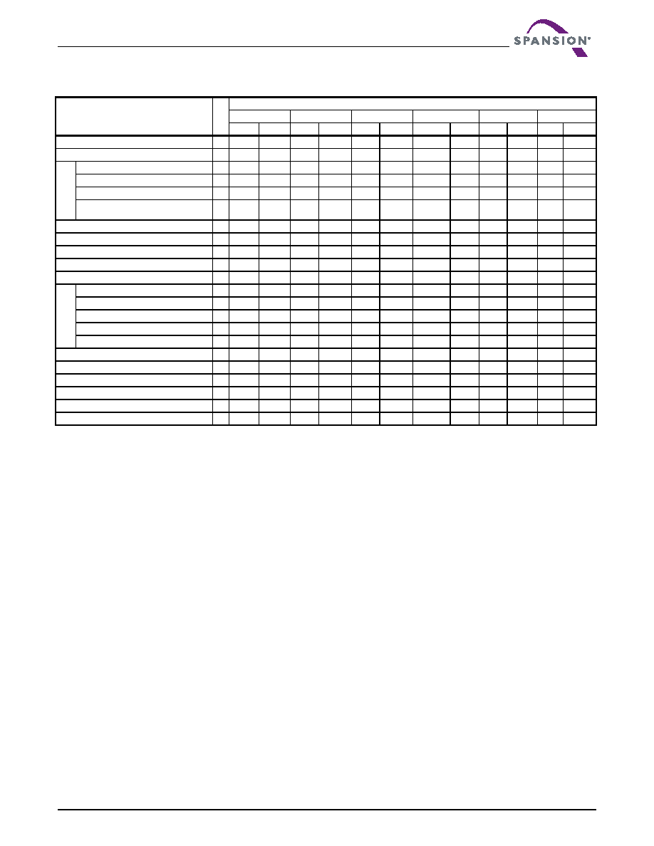
Table 12.3 S29GL-P Memory Array Command Definitions, x8
Command (Notes)
Cyc
le
s
First
Second
Third
Fourth
Fifth
Sixth
Addr
Data
Addr
Data
Addr
Data
Addr
Data
Addr
Data
Addr
Data
Read (6)
1RA
RD
Reset (7)
1
XXX
F0
A
u
toselect
(
,9
)
Manufacturer ID
4
AAA
AA
555
55
AAA
90
X00
01
Device ID (8)
6
AAA
AA
555
55
AAA
90
X02
XX7E
X1C
X1E
Sector Protect Verify (10)
4
AAA
AA
555
55
AAA
90
[SA]X04
Secure Device Verify (11)
4
AAA
AA
555
55
AAA
90
X06
CFI Query (12)
1AA
98
Program
4
AAA
AA
555
55
AAA
A0
PA
PD
Write to Buffer (13)
6
AAA
AA
555
55
SA
25
SA
WC
WBL
PD
WBL
PD
Program Buffer to Flash (confirm)
1
SA
29
Write-to-Buffer-Abort Reset (14)
3
AAA
AA
555
55
555
F0
Unl
o
c
k
By
pass
Enter
3
AAA
AA
555
55
AAA
20
Program (15)
2
XXX
A0
PA
PD
Sector Erase (15)
2
XXX
80
SA
30
Chip Erase (15)
2
XXX
80
XXX
10
Reset (16)
2
XXX
90
XXX
00
Chip Erase
6
AAA
AA
555
55
AAA
80
AAA
AA
555
55
AAA
10
Sector Erase
6
AAA
AA
555
55
AAA
80
AAA
AA
555
55
SA
30
Erase Suspend/Program Suspend (17)
1
XXX
B0
Erase Resume/Program Resume (18)
1
XXX
30
Secured Silicon Sector Entry
3
AAA
AA
555
55
AAA
88
Secured Silicon Sector Exit (19)
4
AAA
AA
555
55
AAA
90
XX
00
Legend
X = Don’t care
RA = Address of the memory to be read.
RD = Data read from location RA during read operation.
PA = Address of the memory location to be programmed. Addresses latch on
the falling edge of the WE# or CE# pulse, whichever happens later.
PD = Data to be programmed at location PA. Data latches on the rising edge
of the WE# or CE# pulse, whichever happens first.
SA = Address of the sector to be verified (in autoselect mode) or erased.
Address bits Amax–A16 uniquely select any sector.
WBL = Write Buffer Location. The address must be within the same write
buffer page as PA.
WC = Word Count is the number of write buffer locations to load minus 1.
Notes
1. See Table 7.1 on page 19 for description of bus operations.
2. All values are in hexadecimal.
3. All bus cycles are write cycles unless otherwise noted.
4. Data bits DQ15-DQ8 are don’t cares for unlock and command cycles.
5. Address bits AMAX:A16 are don’t cares for unlock and command cycles,
unless SA or PA required. (AMAX is the Highest Address pin.).
6. No unlock or command cycles required when reading array data.
7. The Reset command is required to return to reading array data when
device is in the autoselect mode, or if DQ5 goes high (while the device is
providing status data).
8. See Table 7.2 on page 22 for device ID values and definitions.
9. The fourth, fifth, and sixth cycles of the autoselect command sequence are
read cycles.
10. The data is 00h for an unprotected sector and 01h for a protected sector.
See Autoselect on page 21 for more information. This is same as PPB
Status Read except that the protect and unprotect statuses are inverted
here.
11. The data value for DQ7 is “1” for a serialized, protected Secured Silicon
Sector region and “0” for an unserialized, unprotected region. See
Table 7.3 on page 22 for data and definitions.
12. Command is valid when device is ready to read array data or when device
is in autoselect mode.
13. Depending on the number of words written, the total number of cycles may
be from 6 to 69.
14. Command sequence returns device to reading array after being placed in
a Write-to-Buffer-Abort state. Full command sequence is required if
resetting out of abort while in Unlock Bypass mode.
15. The Unlock-Bypass command is required prior to the Unlock-Bypass-
Program command.
16. The Unlock-Bypass-Reset command is required to return to reading array
data when the device is in the unlock bypass mode.
17. The system can read and program/program suspend in non-erasing
sectors, or enter the autoselect mode, when in the Erase Suspend mode.
The Erase Suspend command is valid only during a sector erase
operation.
18. The Erase Resume/Program Resume command is valid only during the
Erase Suspend/Program Suspend modes.
19. The Exit command returns the device to reading the array.
相關(guān)PDF資料 |
PDF描述 |
|---|---|
| S29GL128P10TFIV10 | 3.0 Volt-only Page Mode Flash Memory featuring 90 nm MirrorBit Process Technology |
| S29GL032N90BFI32 | 2M X 16 FLASH 3V PROM, 90 ns, PBGA48 |
| S2A | SURFACE MOUNT RECTIFIER |
| S2B | SURFACE MOUNT RECTIFIER |
| S2C1R-1-5-H | 4000 MHz - 8000 MHz RF/MICROWAVE SGL POLE DOUBLE THROW SWITCH, 1.7 dB INSERTION LOSS |
相關(guān)代理商/技術(shù)參數(shù) |
參數(shù)描述 |
|---|---|
| S29GL128P11FAI010 | 制造商:Spansion 功能描述:FLASH PARALLEL 3V/3.3V 128MBIT 16MX8/8MX16 110NS 64BGA - Trays |
| S29GL128P11FAI010A | 制造商:Spansion 功能描述: |
| S29GL128P11FAI020 | 功能描述:閃存 128MB 2.7-3.6V 110ns Parallel NOR 閃存 RoHS:否 制造商:ON Semiconductor 數(shù)據(jù)總線寬度:1 bit 存儲(chǔ)類型:Flash 存儲(chǔ)容量:2 MB 結(jié)構(gòu):256 K x 8 定時(shí)類型: 接口類型:SPI 訪問時(shí)間: 電源電壓-最大:3.6 V 電源電壓-最小:2.3 V 最大工作電流:15 mA 工作溫度:- 40 C to + 85 C 安裝風(fēng)格:SMD/SMT 封裝 / 箱體: 封裝:Reel |
| S29GL128P11FAIV10 | 制造商:Spansion 功能描述:FLASH PARALLEL 3V/3.3V 128MBIT 16MX8/8MX16 110NS 64BGA - Trays |
| S29GL128P11FAIV20 | 制造商:Spansion 功能描述:FLASH PARALLEL 3V/3.3V 128MBIT 16MX8/8MX16 110NS 64BGA - Trays |
發(fā)布緊急采購,3分鐘左右您將得到回復(fù)。