- 您現(xiàn)在的位置:買賣IC網(wǎng) > PDF目錄299877 > S29GL128P10TFIR10 (SPANSION LLC) 3.0 Volt-only Page Mode Flash Memory featuring 90 nm MirrorBit Process Technology PDF資料下載
參數(shù)資料
| 型號: | S29GL128P10TFIR10 |
| 廠商: | SPANSION LLC |
| 元件分類: | PROM |
| 英文描述: | 3.0 Volt-only Page Mode Flash Memory featuring 90 nm MirrorBit Process Technology |
| 中文描述: | 128M X 1 FLASH 3V PROM, 100 ns, PDSO56 |
| 封裝: | 20 X 14 MM, LEAD FREE, MO-142EC, TSOP-56 |
| 文件頁數(shù): | 35/80頁 |
| 文件大?。?/td> | 2706K |
| 代理商: | S29GL128P10TFIR10 |
第1頁第2頁第3頁第4頁第5頁第6頁第7頁第8頁第9頁第10頁第11頁第12頁第13頁第14頁第15頁第16頁第17頁第18頁第19頁第20頁第21頁第22頁第23頁第24頁第25頁第26頁第27頁第28頁第29頁第30頁第31頁第32頁第33頁第34頁當(dāng)前第35頁第36頁第37頁第38頁第39頁第40頁第41頁第42頁第43頁第44頁第45頁第46頁第47頁第48頁第49頁第50頁第51頁第52頁第53頁第54頁第55頁第56頁第57頁第58頁第59頁第60頁第61頁第62頁第63頁第64頁第65頁第66頁第67頁第68頁第69頁第70頁第71頁第72頁第73頁第74頁第75頁第76頁第77頁第78頁第79頁第80頁
40
S29GL-P MirrorBit Flash Family
S29GL-P_00_A12 November 20, 2009
Da ta
Sh e e t
Notes
1. DQ5 switches to 1 when an Embedded Program, Embedded Erase, or Write-to-Buffer operation has exceeded the maximum timing limits.
Refer toDQ5: Exceeded Timing Limits on page 39 for more information.
2. DQ7 and DQ2 require a valid address when reading status information. Refer to the appropriate subsection for further details.
3. The Data# Polling algorithm should be used to monitor the last loaded write-buffer address location.
4. DQ1 switches to 1 when the device has aborted the write-to-buffer operation
7.9
Writing Commands/Command Sequences
During a write operation, the system must drive CE# and WE# to VIL and OE# to VIH when providing an
address, command, and data. Addresses are latched on the last falling edge of WE# or CE#, while data is
latched on the 1st rising edge of WE# or CE#. An erase operation can erase one sector, multiple sectors, or
the entire device. Table 6.1 – Table 6.4 indicate the address space that each sector occupies. The device
address space is divided into uniform 64KW/128KB sectors. A sector address is the set of address bits
required to uniquely select a sector. ICC2 in “DC Characteristics” represents the active current specification for
the write mode. “AC Characteristics” contains timing specification tables and timing diagrams for write
operations.
7.9.1
RY/BY#
The RY/BY# is a dedicated, open-drain output pin that indicates whether an Embedded Algorithm is in
progress or complete. The RY/BY# status is valid after the rising edge of the final WE# pulse in the command
sequence. Since RY/BY# is an open-drain output, several RY/BY# pins can be tied together in parallel with a
pull-up resistor to VCC. This feature allows the host system to detect when data is ready to be read by simply
monitoring the RY/BY# pin, which is a dedicated output and controlled by CE# (not OE#).
7.9.2
Hardware Reset
The RESET# input provides a hardware method of resetting the device to reading array data. When RESET#
is driven low for at least a period of tRP (RESET# Pulse Width), the device immediately terminates any
operation in progress, tristates all outputs, resets the configuration register, and ignores all read/write
commands for the duration of the RESET# pulse. The device also resets the internal state machine to reading
array data.
To ensure data integrity Program/Erase operations that were interrupted should be reinitiated once the device
is ready to accept another command sequence.
When RESET# is held at VSS, the device draws VCC reset current (ICC5). If RESET# is held at VIL, but not at
VSS, the standby current is greater. RESET# may be tied to the system reset circuitry which enables the
system to read the boot-up firmware from the Flash memory upon a system reset. See Figure 11.7
on page 59 and Figure 11.8 on page 60 for timing diagrams.
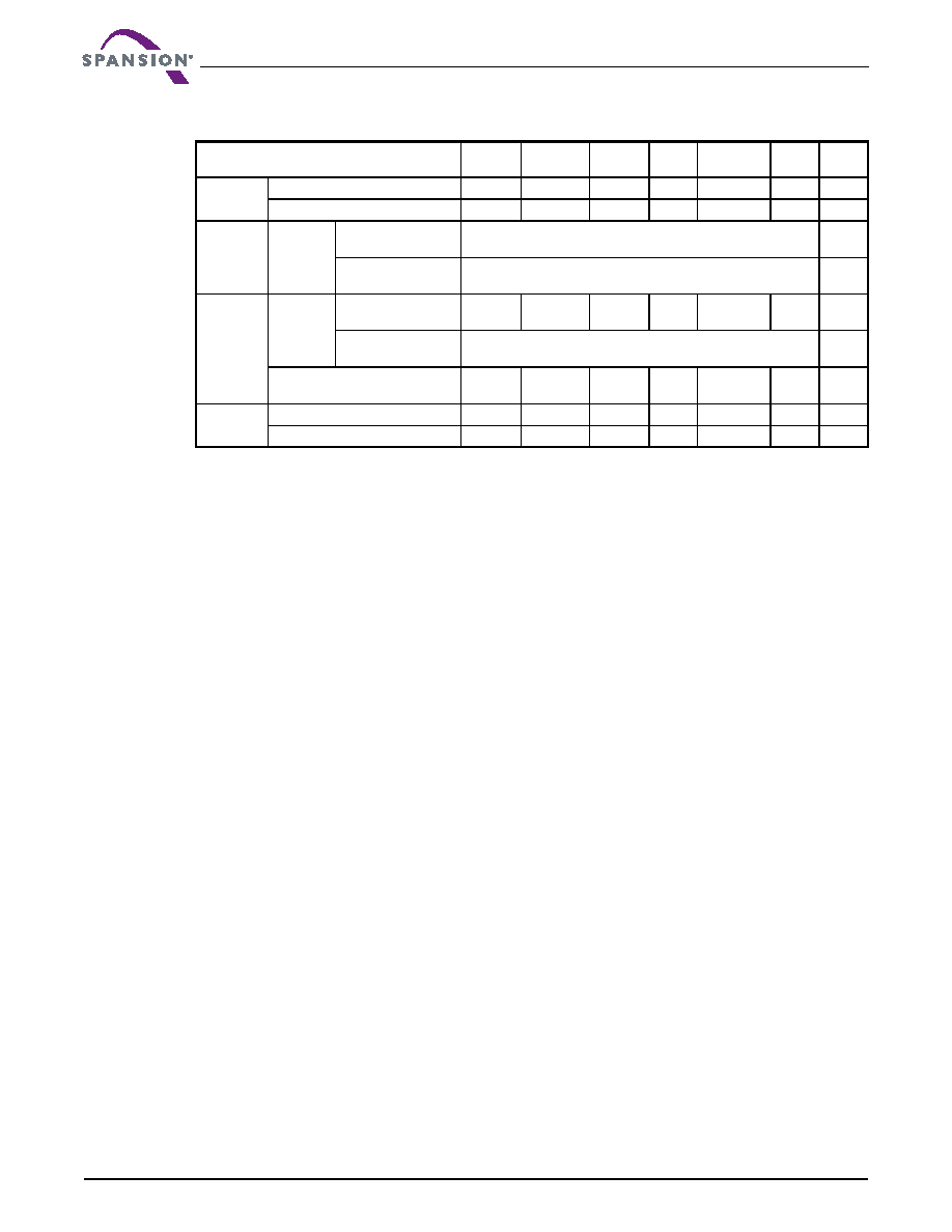
Table 7.17 Write Operation Status
Status
DQ7
DQ6
DQ5
DQ3
DQ2
DQ1
RY/
BY#
Standard
Mode
Embedded Program Algorithm
DQ7#
Toggle
0
N/A
No toggle
0
Embedded Erase Algorithm
0
Toggle
0
1
Toggle
N/A
0
Program
Suspend
Mode
Program-
Suspend
Read
Program-Suspended
Sector
Invalid (not allowed)
1
Non-Program
Suspended Sector
Data
1
Erase
Suspend
Mode
Erase-
Suspend
Read
Erase-Suspended
Sector
1
No toggle
0
N/A
Toggle
N/A
1
Non-Erase
Suspended Sector
Data
1
Erase-Suspend-Program
(Embedded Program)
DQ7#
Toggle
0
N/A
0
Write-to-
Buffer
Busy (Note 3)
DQ7#
Toggle
0
N/A
0
Abort (Note 4)
DQ7#
Toggle
0
N/A
1
0
相關(guān)PDF資料 |
PDF描述 |
|---|---|
| S29GL128P10TFIV10 | 3.0 Volt-only Page Mode Flash Memory featuring 90 nm MirrorBit Process Technology |
| S29GL032N90BFI32 | 2M X 16 FLASH 3V PROM, 90 ns, PBGA48 |
| S2A | SURFACE MOUNT RECTIFIER |
| S2B | SURFACE MOUNT RECTIFIER |
| S2C1R-1-5-H | 4000 MHz - 8000 MHz RF/MICROWAVE SGL POLE DOUBLE THROW SWITCH, 1.7 dB INSERTION LOSS |
相關(guān)代理商/技術(shù)參數(shù) |
參數(shù)描述 |
|---|---|
| S29GL128P11FAI010 | 制造商:Spansion 功能描述:FLASH PARALLEL 3V/3.3V 128MBIT 16MX8/8MX16 110NS 64BGA - Trays |
| S29GL128P11FAI010A | 制造商:Spansion 功能描述: |
| S29GL128P11FAI020 | 功能描述:閃存 128MB 2.7-3.6V 110ns Parallel NOR 閃存 RoHS:否 制造商:ON Semiconductor 數(shù)據(jù)總線寬度:1 bit 存儲類型:Flash 存儲容量:2 MB 結(jié)構(gòu):256 K x 8 定時類型: 接口類型:SPI 訪問時間: 電源電壓-最大:3.6 V 電源電壓-最小:2.3 V 最大工作電流:15 mA 工作溫度:- 40 C to + 85 C 安裝風(fēng)格:SMD/SMT 封裝 / 箱體: 封裝:Reel |
| S29GL128P11FAIV10 | 制造商:Spansion 功能描述:FLASH PARALLEL 3V/3.3V 128MBIT 16MX8/8MX16 110NS 64BGA - Trays |
| S29GL128P11FAIV20 | 制造商:Spansion 功能描述:FLASH PARALLEL 3V/3.3V 128MBIT 16MX8/8MX16 110NS 64BGA - Trays |
發(fā)布緊急采購,3分鐘左右您將得到回復(fù)。