- 您現(xiàn)在的位置:買賣IC網(wǎng) > PDF目錄299877 > S1C60L09D 4-BIT, MROM, 0.08 MHz, MICROCONTROLLER, UUC70 PDF資料下載
參數(shù)資料
| 型號: | S1C60L09D |
| 元件分類: | 微控制器/微處理器 |
| 英文描述: | 4-BIT, MROM, 0.08 MHz, MICROCONTROLLER, UUC70 |
| 封裝: | DIE-70 |
| 文件頁數(shù): | 49/62頁 |
| 文件大小: | 476K |
| 代理商: | S1C60L09D |
第1頁第2頁第3頁第4頁第5頁第6頁第7頁第8頁第9頁第10頁第11頁第12頁第13頁第14頁第15頁第16頁第17頁第18頁第19頁第20頁第21頁第22頁第23頁第24頁第25頁第26頁第27頁第28頁第29頁第30頁第31頁第32頁第33頁第34頁第35頁第36頁第37頁第38頁第39頁第40頁第41頁第42頁第43頁第44頁第45頁第46頁第47頁第48頁當(dāng)前第49頁第50頁第51頁第52頁第53頁第54頁第55頁第56頁第57頁第58頁第59頁第60頁第61頁第62頁
CHAPTER 6: ELECTRICAL CHARACTERISTICS
S1C60N09 TECHNICAL MANUAL
EPSON
47
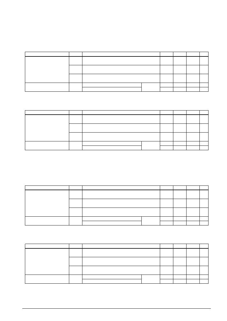
S1C60L09 (Crystal oscillation)
4.5 V LCD panel, 1/4, 1/3, 1/2 duty, 1/3 bias (VL1 is shorted to VSS inside the IC)
Normal mode
Item
LCD drive voltage
Current consumption
Unless otherwise specified:
VDD=0V, VSS=-1.5V, fOSC=32.768kHz, Ta=25
°C, CG=25pF, VS1/VL1–VL3 are internal voltage, C1–C4=0.1F
Symbol
VL1
VL2
VL3
IOP
Unit
V
A
Max.
2VL1
×0.9
3VL1
×0.9
2.5
5.0
Typ.
VSS
1.0
2.5
Min.
2VL1
- 0.1
3VL1
- 0.1
Condition
Connect 1 M
load resistor between VDD and VL1
(without panel load)
Connect 1 M
load resistor between VDD and VL2
(without panel load)
Connect 1 M
load resistor between VDD and VL3
(without panel load)
During HALT
Without
During execution
panel load
Heavy load protection mode
Item
LCD drive voltage
Current consumption
Unless otherwise specified:
VDD=0V, VSS=-1.5V, fOSC=32.768kHz, Ta=25
°C, CG=25pF, VS1/VL1–VL3 are internal voltage, C1–C4=0.1F
Symbol
VL1
VL2
VL3
IOP
Unit
V
A
Max.
2VL1
×0.85
3VL1
×0.85
5.5
10.0
Typ.
VSS
2.0
5.5
Min.
2VL1
- 0.1
3VL1
- 0.1
Condition
Connect 1 M
load resistor between VDD and VL1
(without panel load)
Connect 1 M
load resistor between VDD and VL2
(without panel load)
Connect 1 M
load resistor between VDD and VL3
(without panel load)
During HALT
Without
During execution
panel load
3 V LCD panel, 1/4, 1/3, 1/2 duty, 1/2 bias (VL1 is shorted to VSS inside the IC and VL1 is shorted
to VL2 outside the IC)
Normal mode
Item
LCD drive voltage
Current consumption
Unless otherwise specified:
VDD=0V, VSS=-1.5V, fOSC=32.768kHz, Ta=25
°C, CG=25pF, VS1/VL1–VL3 are internal voltage, C1–C3=0.1F
Symbol
VL1
VL2
VL3
IOP
Unit
V
A
Max.
2VL1
×0.9
2.5
5.0
Typ.
VSS
1.0
2.5
Min.
2VL1
- 0.1
Condition
Connect 1 M
load resistor between VDD and VL1
(without panel load)
Connect 1 M
load resistor between VDD and VL2
(without panel load)
Connect 1 M
load resistor between VDD and VL3
(without panel load)
During HALT
Without
During execution
panel load
Heavy load protection mode
Item
LCD drive voltage
Current consumption
Unless otherwise specified:
VDD=0V, VSS=-1.5V, fOSC=32.768kHz, Ta=25
°C, CG=25pF, VS1/VL1–VL3 are internal voltage, C1–C3=0.1F
Symbol
VL1
VL2
VL3
IOP
Unit
V
A
Max.
2VL1
×0.85
5.5
10.0
Typ.
VSS
2.0
5.5
Min.
2VL1
- 0.1
Condition
Connect 1 M
load resistor between VDD and VL1
(without panel load)
Connect 1 M
load resistor between VDD and VL2
(without panel load)
Connect 1 M
load resistor between VDD and VL3
(without panel load)
During HALT
Without
During execution
panel load
相關(guān)PDF資料 |
PDF描述 |
|---|---|
| S1C63358F | 4-BIT, MROM, 4.1 MHz, MICROCONTROLLER, PQFP100 |
| S1D13503F00A | 1024 X 768 PIXELS CRT OR FLAT PNL GRPH DSPL CTLR, PQFP100 |
| S1DGPC | SLIDE SWITCH, SPDT, LATCHED, 0.05A, 48VDC, THROUGH HOLE-STRAIGHT |
| S1F | 1.2 A, 50 V, SCR, TO-92 |
| S2A | 1.5 A, 100 V, SCR, TO-92 |
相關(guān)代理商/技術(shù)參數(shù) |
參數(shù)描述 |
|---|---|
| S1C60L16 | 制造商:EPSON 制造商全稱:EPSON 功能描述:4-bit Single Chip Microcomputer |
| S1C60N05 | 制造商:EPSON 制造商全稱:EPSON 功能描述:4-bit Single Chip Microcomputer |
| S1C60N08 | 制造商:EPSON 制造商全稱:EPSON 功能描述:4-bit Single Chip Microcomputer |
| S1C60N16 | 制造商:EPSON 制造商全稱:EPSON 功能描述:4-bit Single Chip Microcomputer |
| S1C60R08 | 制造商:EPSON 制造商全稱:EPSON 功能描述:4-bit Single Chip Microcomputer |
發(fā)布緊急采購,3分鐘左右您將得到回復(fù)。