- 您現(xiàn)在的位置:買賣IC網 > PDF目錄299790 > PSD854F2A-90UT (STMICROELECTRONICS) 256K X 8 FLASH, 27 I/O, PIA-GENERAL PURPOSE, PQFP64 PDF資料下載
參數資料
| 型號: | PSD854F2A-90UT |
| 廠商: | STMICROELECTRONICS |
| 元件分類: | 微控制器/微處理器 |
| 英文描述: | 256K X 8 FLASH, 27 I/O, PIA-GENERAL PURPOSE, PQFP64 |
| 封裝: | ROHS COMPLIANT, TQFP-64 |
| 文件頁數: | 71/128頁 |
| 文件大小: | 1045K |
| 代理商: | PSD854F2A-90UT |
第1頁第2頁第3頁第4頁第5頁第6頁第7頁第8頁第9頁第10頁第11頁第12頁第13頁第14頁第15頁第16頁第17頁第18頁第19頁第20頁第21頁第22頁第23頁第24頁第25頁第26頁第27頁第28頁第29頁第30頁第31頁第32頁第33頁第34頁第35頁第36頁第37頁第38頁第39頁第40頁第41頁第42頁第43頁第44頁第45頁第46頁第47頁第48頁第49頁第50頁第51頁第52頁第53頁第54頁第55頁第56頁第57頁第58頁第59頁第60頁第61頁第62頁第63頁第64頁第65頁第66頁第67頁第68頁第69頁第70頁當前第71頁第72頁第73頁第74頁第75頁第76頁第77頁第78頁第79頁第80頁第81頁第82頁第83頁第84頁第85頁第86頁第87頁第88頁第89頁第90頁第91頁第92頁第93頁第94頁第95頁第96頁第97頁第98頁第99頁第100頁第101頁第102頁第103頁第104頁第105頁第106頁第107頁第108頁第109頁第110頁第111頁第112頁第113頁第114頁第115頁第116頁第117頁第118頁第119頁第120頁第121頁第122頁第123頁第124頁第125頁第126頁第127頁第128頁
PSD8XXFX
PLDS
Doc ID 7833 Rev 7
14
PLDS
The PLDs bring programmable logic functionality to the PSD. After specifying the logic for
the PLDs using the PSDabel tool in PSDsoft Express, the logic is programmed into the
device and available upon Power-up.
The PSD contains two PLDs: the Decode PLD (DPLD), and the Complex PLD (CPLD). The
PLDs are briefly discussed in the next few paragraphs, and in more detail in Section 14.2:
configuration of the PLDs.
The DPLD performs address decoding for Select signals for internal components, such as
memory, registers, and I/O ports.
The CPLD can be used for logic functions, such as loadable counters and shift registers,
state machines, and encoding and decoding logic. These logic functions can be constructed
using the 16 Output macrocells (OMC), 24 input macrocells (IMC), and the AND Array. The
CPLD can also be used to generate External Chip Select (ECS0-ECS2) signals.
The AND Array is used to form product terms. These product terms are specified using
PSDabel. An input bus consisting of 73 signals is connected to the PLDs. The signals are
shown in Table 15.
14.1
The Turbo Bit in PSD
The PLDs in the PSD can minimize power consumption by switching off when inputs remain
unchanged for an extended time of about 70ns. Resetting the Turbo Bit to '0' (Bit 3 of
PMMR0) automatically places the PLDs into standby if no inputs are changing. Turning the
Turbo mode off increases propagation delays while reducing power consumption. See
Section 17: Power management on how to set the Turbo Bit.
Additionally, five bits are available in PMMR2 to block MCU control signals from entering the
PLDs. This reduces power consumption and can be used only when these MCU control
signals are not used in PLD logic equations.
Each of the two PLDs has unique characteristics suited for its applications. They are
described in the following sections.
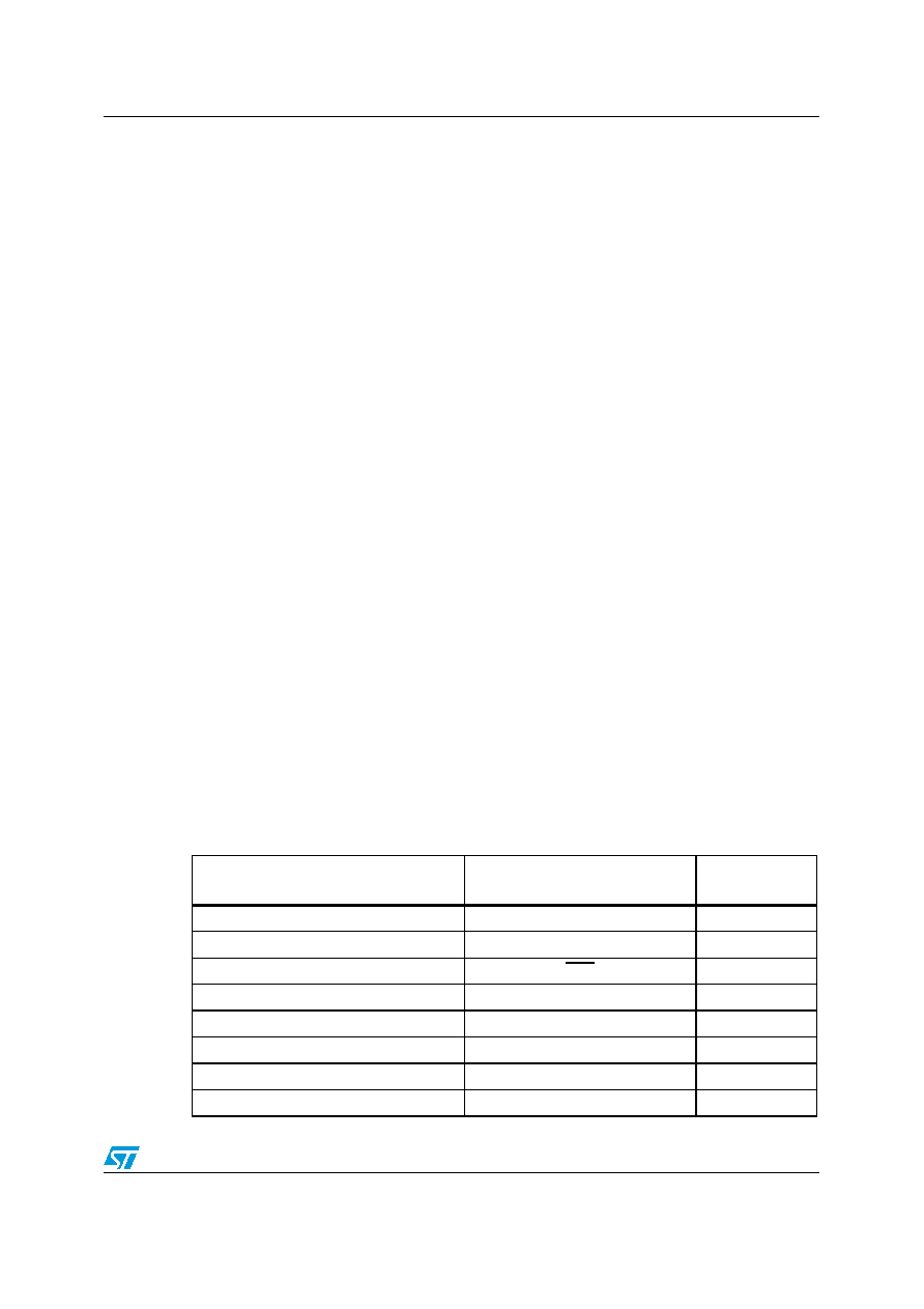
Table 15.
DPLD and CPLD inputs
Input source
Input name
Number of
signals
MCU address bus(1)
A15-A0
16
MCU control signals
CNTL2-CNTL0
3
Reset
RST
1
Power-down
PDN
1
Port A input macrocells
PA7-PA0
8
Port B input macrocells
PB7-PB0
8
Port C input macrocells
PC7-PC0
8
Port D inputs
PD2-PD0
3
相關PDF資料 |
PDF描述 |
|---|---|
| PSH665-FREQ-OUT1 | VCXO, SINE OUTPUT, 465 MHz - 865 MHz |
| PSM3-022K | 1 ELEMENT, 0.022 uH, GENERAL PURPOSE INDUCTOR, SMD |
| PSM3-068K | 1 ELEMENT, 0.068 uH, GENERAL PURPOSE INDUCTOR, SMD |
| PSM3-120K | 1 ELEMENT, 0.12 uH, GENERAL PURPOSE INDUCTOR, SMD |
| PSM3-121K | 1 ELEMENT, 1.2 uH, GENERAL PURPOSE INDUCTOR, SMD |
相關代理商/技術參數 |
參數描述 |
|---|---|
| PSD854F2V-12JI | 功能描述:CPLD - 復雜可編程邏輯器件 3.0V 2M 120ns RoHS:否 制造商:Lattice 系列: 存儲類型:EEPROM 大電池數量:128 最大工作頻率:333 MHz 延遲時間:2.7 ns 可編程輸入/輸出端數量:64 工作電源電壓:3.3 V 最大工作溫度:+ 90 C 最小工作溫度:0 C 封裝 / 箱體:TQFP-100 |
| PSD854F2V-12MI | 功能描述:CPLD - 復雜可編程邏輯器件 3.0V 2M 120ns RoHS:否 制造商:Lattice 系列: 存儲類型:EEPROM 大電池數量:128 最大工作頻率:333 MHz 延遲時間:2.7 ns 可編程輸入/輸出端數量:64 工作電源電壓:3.3 V 最大工作溫度:+ 90 C 最小工作溫度:0 C 封裝 / 箱體:TQFP-100 |
| PSD854F2V-90J | 功能描述:CPLD - 復雜可編程邏輯器件 3.0V 2M 90ns RoHS:否 制造商:Lattice 系列: 存儲類型:EEPROM 大電池數量:128 最大工作頻率:333 MHz 延遲時間:2.7 ns 可編程輸入/輸出端數量:64 工作電源電壓:3.3 V 最大工作溫度:+ 90 C 最小工作溫度:0 C 封裝 / 箱體:TQFP-100 |
| PSD854F2V-90M | 功能描述:CPLD - 復雜可編程邏輯器件 3.0V 2M 90ns RoHS:否 制造商:Lattice 系列: 存儲類型:EEPROM 大電池數量:128 最大工作頻率:333 MHz 延遲時間:2.7 ns 可編程輸入/輸出端數量:64 工作電源電壓:3.3 V 最大工作溫度:+ 90 C 最小工作溫度:0 C 封裝 / 箱體:TQFP-100 |
| PSD-8M-01 | 制造商:Richco 功能描述:CB SPT REST MNT NAT 8MM SPC |
發(fā)布緊急采購,3分鐘左右您將得到回復。