- 您現(xiàn)在的位置:買賣IC網(wǎng) > PDF目錄379326 > MTD2N40E (MOTOROLA INC) TMOS POWER FET 2.0 AMPERES 400 VOLTS RDS(on) = 3.5 OHM PDF資料下載
參數(shù)資料
| 型號(hào): | MTD2N40E |
| 廠商: | MOTOROLA INC |
| 元件分類: | JFETs |
| 英文描述: | TMOS POWER FET 2.0 AMPERES 400 VOLTS RDS(on) = 3.5 OHM |
| 中文描述: | 2 A, 400 V, 3.5 ohm, N-CHANNEL, Si, POWER, MOSFET |
| 文件頁(yè)數(shù): | 1/10頁(yè) |
| 文件大小: | 268K |
| 代理商: | MTD2N40E |
1
Motorola, Inc. 1995
"!
N–Channel Enhancement–Mode Silicon Gate
This advanced high voltage TMOS E–FET is designed to
withstand high energy in the avalanche and switch efficiently. This
new high energy device also offers a drain–to–soure diode with fast
recovery time. Designed for high voltage, high speed switching
applications such as power supplies, PWM motor controls and
other inductive loads, the avalanche energy capability is specified
to eliminate the guesswork in designs where inductive loads are
switched and offer additional safety margin against unexpected
voltage transients.
Robust High Voltage Termination
Avalanche Energy Specified
Source–to–Drain Diode Recovery Time Comparable to a
Discrete Fast Recovery Diode
Diode is Characterized for Use in Bridge Circuits
IDSS and VDS(on) Specified at Elevated Temperature
Surface Mount Package Available in 16 mm, 13–inch/2500
Unit Tape & Reel, Add –T4 Suffix to Part Number
Replaces MTD1N40E
MAXIMUM RATINGS
(TC = 25
°
C unless otherwise noted)
Rating
Symbol
Value
Unit
Drain–Source Voltage
VDSS
VDGR
VGS
VGSM
400
Vdc
Drain–Gate Voltage (RGS = 1.0 M
)
Gate–Source Voltage — Continuous
Gate–Source Voltage
— Non–Repetitive (tp
≤
10 ms)
400
Vdc
±
20
±
40
Vdc
Vpk
Drain Current — Continuous @ TC = 25
°
C
Drain Current
— Continuous @ 100
°
C
Drain Current
— Single Pulse (tp
≤
10
μ
s)
Total Power Dissipation @ TC = 25
°
C
Derate above 25
°
C
Total Power Dissipation @ TC = 25
°
C, when mounted to minimum recommended pad size
ID
ID
IDM
2.0
1.5
6.0
Adc
Apk
PD
40
0.32
1.75
Watts
W/
°
C
Watts
Operating and Storage Temperature Range
TJ, Tstg
EAS
–55 to 150
°
C
Single Pulse Drain–to–Source Avalanche Energy — Starting TJ = 25
°
C
(VDD = 100 Vdc, VGS = 10 Vdc, IL = 3.0 Apk, L = 10 mH, RG = 25
)
45
mJ
Thermal Resistance — Junction to Case
Thermal Resistance
— Junction to Ambient
Thermal Resistance
— Junction to Ambient, when mounted to minimum recommended pad size
R
θ
JC
R
θ
JA
R
θ
JA
TL
3.13
100
71.4
°
C/W
Maximum Temperature for Soldering Purposes, 1/8
″
from case for 10 seconds
260
°
C
Designer’s Data for “Worst Case” Conditions
— The Designer’s Data Sheet permits the design of most circuits entirely from the information presented. SOA Limit
curves — representing boundaries on device characteristics — are given to facilitate “worst case” design.
E–FET and Designer’s are trademarks of Motorola, Inc. TMOS is a registered trademark of Motorola, Inc.
Thermal Clad is a trademark of the Bergquist Company.
Preferred
devices are Motorola recommended choices for future use and best overall value.
Order this document
by MTD2N40E/D
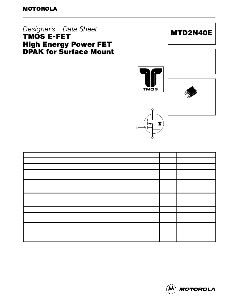
SEMICONDUCTOR TECHNICAL DATA
D
S
G
CASE 369A–13, Style 2
DPAK
TMOS POWER FET
2.0 AMPERES
400 VOLTS
RDS(on) = 3.5 OHM
Motorola Preferred Device
相關(guān)PDF資料 |
PDF描述 |
|---|---|
| MTD2N50E | TMOS POWER FET 2.0 AMPERES 500 VOLTS RDS(on) = 3.6 OHM |
| MTD3N25E | TMOS POWER FET 3 AMPERES 250 VOLTS RDS(on) = 1.4 OHM |
| MTD4N20E | TMOS POWER FET 4.0 AMPERES 200 VOLTS RDS(on) = 1.2 OHM |
| MTP27N10E | LASER MODULE 635NM 4.2MW MVP |
| MTP50P03HDL | TMOS POWER FET LOGIC LEVEL 50 AMPERES 30 VOLTS RDS(on) = 0.025 OHM |
相關(guān)代理商/技術(shù)參數(shù) |
參數(shù)描述 |
|---|---|
| MTD2N40ET4 | 制造商:Rochester Electronics LLC 功能描述:- Bulk |
| MTD2N50 | 制造商:MOTOROLA 制造商全稱:Motorola, Inc 功能描述:POWER FIELD EFFECT TRANSISTOR N-CHANNEL ENHANCEMENT-MODE SILICON GATE DPAK FOR SURFACE MOUNT OR INSERTION MOUNT |
| MTD2N50E | 制造商:MOTOROLA 制造商全稱:Motorola, Inc 功能描述:TMOS POWER FET 2.0 AMPERES 500 VOLTS RDS(on) = 3.6 OHM |
| MTD2N50E1 | 制造商:Rochester Electronics LLC 功能描述:- Bulk |
| MTD3010N | 功能描述:PHOTO DIODE 900NM DOME CLR TO-18 RoHS:是 類別:傳感器,轉(zhuǎn)換器 >> 光學(xué) - 光電檢測(cè)器 - 光電二極管 系列:- 標(biāo)準(zhǔn)包裝:1 系列:- 波長(zhǎng):850nm 顏色 - 增強(qiáng)型:- 光譜范圍:400nm ~ 1100nm 二極管類型:引腳 nm 下響應(yīng)率:0.62 A/W @ 850nm 響應(yīng)時(shí)間:5ns 電壓 - (Vr)(最大):50V 電流 - 暗(標(biāo)準(zhǔn)):1nA 有效面積:1mm² 視角:150° 工作溫度:-40°C ~ 100°C 封裝/外殼:徑向,5mm 直徑(T 1 3/4) 其它名稱:475-2649-6 |
發(fā)布緊急采購(gòu),3分鐘左右您將得到回復(fù)。