- 您現(xiàn)在的位置:買賣IC網(wǎng) > PDF目錄379326 > MTB75N03HDL (MOTOROLA INC) TMOS POWER FET LOGIC LEVEL 75 AMPERES 25 VOLTS PDF資料下載
參數(shù)資料
| 型號(hào): | MTB75N03HDL |
| 廠商: | MOTOROLA INC |
| 元件分類: | JFETs |
| 英文描述: | TMOS POWER FET LOGIC LEVEL 75 AMPERES 25 VOLTS |
| 中文描述: | 75 A, 30 V, 0.007 ohm, N-CHANNEL, Si, POWER, MOSFET |
| 文件頁(yè)數(shù): | 6/12頁(yè) |
| 文件大?。?/td> | 304K |
| 代理商: | MTB75N03HDL |
6
Motorola TMOS Power MOSFET Transistor Device Data
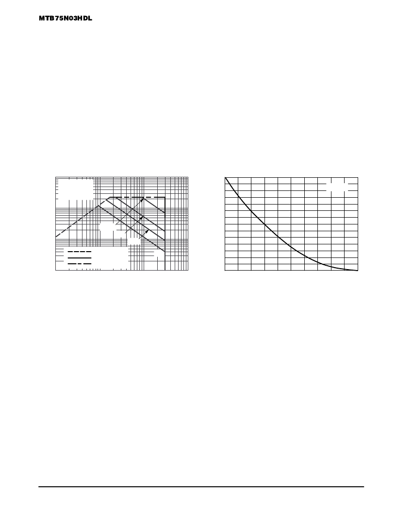
SAFE OPERATING AREA
The Forward Biased Safe Operating Area curves define
the maximum simultaneous drain–to–source voltage and
drain current that a transistor can handle safely when it is for-
ward biased. Curves are based upon maximum peak junc-
tion temperature and a case temperature (TC) of 25
°
C. Peak
repetitive pulsed power limits are determined by using the
thermal response data in conjunction with the procedures
discussed in AN569, “Transient Thermal Resistance – Gen-
eral Data and Its Use.”
Switching between the off–state and the on–state may tra-
verse any load line provided neither rated peak current (IDM)
nor rated voltage (VDSS) is exceeded, and that the transition
time (tr, tf) does not exceed 10
μ
s. In addition the total power
averaged over a complete switching cycle must not exceed
(TJ(MAX) – TC)/(R
θ
JC).
A power MOSFET designated E–FET can be safely used
in switching circuits with unclamped inductive loads. For reli-
able operation, the stored energy from circuit inductance dis-
sipated in the transistor while in avalanche must be less than
the rated limit and must be adjusted for operating conditions
differing from those specified. Although industry practice is to
rate in terms of energy, avalanche energy capability is not a
constant. The energy rating decreases non–linearly with an
increase of peak current in avalanche and peak junction tem-
perature.
Although many E–FETs can withstand the stress of drain–
to–source avalanche at currents up to rated pulsed current
(IDM), the energy rating is specified at rated continuous cur-
rent (ID), in accordance with industry custom. The energy rat-
ing must be derated for temperature as shown in the
accompanying graph (Figure 13). Maximum energy at cur-
rents below rated continuous ID can safely be assumed to
equal the values indicated.
Figure 11. Maximum Rated Forward Biased
Safe Operating Area
Figure 12. Maximum Avalanche Energy versus
Starting Junction Temperature
0.1
100
RDS(on) LIMIT
THERMAL LIMIT
PACKAGE LIMIT
10
VGS = 20 V
SINGLE PULSE
TC = 25
°
C
1
10
100
1000
1
dc
100
μ
s
1 ms
10 ms
TJ, STARTING JUNCTION TEMPERATURE (
°
C)
EA
VDS, DRAIN–TO–SOURCE VOLTAGE (VOLTS)
A
I
25
50
75
100
125
ID = 75 A
150
80
280
200
160
120
240
40
0
相關(guān)PDF資料 |
PDF描述 |
|---|---|
| MTB8N50E | TMOS POWER FET 8.0 AMPERES 500 VOLTS |
| MTD1P50E | TMOS POWER FET 1.0 AMPERES 500 VOLTS 15 OHM |
| MTD2N40E | TMOS POWER FET 2.0 AMPERES 400 VOLTS RDS(on) = 3.5 OHM |
| MTD2N50E | TMOS POWER FET 2.0 AMPERES 500 VOLTS RDS(on) = 3.6 OHM |
| MTD3N25E | TMOS POWER FET 3 AMPERES 250 VOLTS RDS(on) = 1.4 OHM |
相關(guān)代理商/技術(shù)參數(shù) |
參數(shù)描述 |
|---|---|
| MTB75N05HD | 制造商:MOTOROLA 制造商全稱:Motorola, Inc 功能描述:TMOS POWER FET 75 AMPERES 50 VOLTS |
| MTB75N05HDT4 | 功能描述:MOSFET N-CH 50V 75A D2PAK-3 RoHS:否 類別:分離式半導(dǎo)體產(chǎn)品 >> FET - 單 系列:- 標(biāo)準(zhǔn)包裝:1,000 系列:MESH OVERLAY™ FET 型:MOSFET N 通道,金屬氧化物 FET 特點(diǎn):邏輯電平門 漏極至源極電壓(Vdss):200V 電流 - 連續(xù)漏極(Id) @ 25° C:18A 開態(tài)Rds(最大)@ Id, Vgs @ 25° C:180 毫歐 @ 9A,10V Id 時(shí)的 Vgs(th)(最大):4V @ 250µA 閘電荷(Qg) @ Vgs:72nC @ 10V 輸入電容 (Ciss) @ Vds:1560pF @ 25V 功率 - 最大:40W 安裝類型:通孔 封裝/外殼:TO-220-3 整包 供應(yīng)商設(shè)備封裝:TO-220FP 包裝:管件 |
| MTB75N06 | 制造商:MOTOROLA 制造商全稱:Motorola, Inc 功能描述:TMOS POWER FET 75 AMPERES 60 VOLTS |
| MTB75N06HD | 制造商:ON Semiconductor 功能描述:Trans MOSFET N-CH 60V 75A 3-Pin(2+Tab) D2PAK Rail |
| MTB7671 | 制造商:Megger 功能描述:METER TEST BOX |
發(fā)布緊急采購(gòu),3分鐘左右您將得到回復(fù)。