- 您現(xiàn)在的位置:買賣IC網(wǎng) > PDF目錄65818 > MSP50C614PJM (TEXAS INSTRUMENTS INC) 0-BIT, 12.32 MHz, MIXED DSP, PQFP100 PDF資料下載
參數(shù)資料
| 型號: | MSP50C614PJM |
| 廠商: | TEXAS INSTRUMENTS INC |
| 元件分類: | 數(shù)字信號處理 |
| 英文描述: | 0-BIT, 12.32 MHz, MIXED DSP, PQFP100 |
| 封裝: | PLASTIC, QFP-100 |
| 文件頁數(shù): | 5/9頁 |
| 文件大?。?/td> | 122K |
| 代理商: | MSP50C614PJM |
MSP50C614
MIXED-SIGNAL PROCESSOR
SPSS023C – DECEMBER 1999 – REVISED FEBRUARY 2001
5
POST OFFICE BOX 655303
DALLAS, TEXAS 75265
absolute maximum ratings over operating free-air temperature range (unless otherwise noted)
Supply voltage, VDD (see Note 1)
– 0.3 to 7 V
. . . . . . . . . . . . . . . . . . . . . . . . . . . . . . . . . . . . . . . . . . . . . . . . . . . . . .
Supply current, IDD (see Note 2)
35 mA
. . . . . . . . . . . . . . . . . . . . . . . . . . . . . . . . . . . . . . . . . . . . . . . . . . . . . . . . . . .
Input voltage range, VI (see Note 1)
– 0.3 to VDD + 0.3 V
. . . . . . . . . . . . . . . . . . . . . . . . . . . . . . . . . . . . . . . . . . . .
Output voltage range, VO (see Note 1)
– 0.3 to VDD + 0.3 V
. . . . . . . . . . . . . . . . . . . . . . . . . . . . . . . . . . . . . . . . .
Storage temperature range, TA
– 30
°C to 125°C
. . . . . . . . . . . . . . . . . . . . . . . . . . . . . . . . . . . . . . . . . . . . . . . . . . . .
Stresses beyond those listed under “absolute maximum ratings” may cause permanent damage to the device. These are stress ratings only, and
functional operation of the device at these or any other conditions beyond those indicated under “recommended operating conditions” is not
implied. Exposure to absolute-maximum-rated conditions for extended periods may affect device reliability.
NOTES:
1. Unless otherwise noted, all voltages are measured with respect to VSS .
2. The total supply current includes the current out of all the I/O pins as well as the operating current of the device.
recommended operating conditions
MIN
MAX
UNIT
Supply voltage (with respect to VSS), VDD
3
5.2
V
CPU clock rate (as programmed), f(CPU)
64
12,320
kHz
Load resistance between DACP and DACM, R(DAC)
32
Operating free-air temperature, TA
Device functionality
0
70
°C
timing requirements
MIN
MAX
UNIT
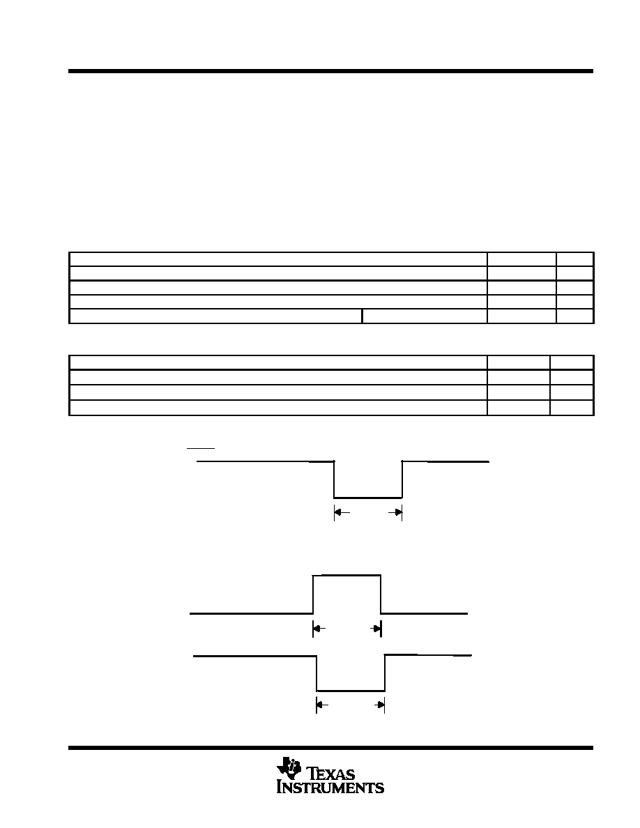
t(RESET)
Reset low pulse width, while VDD is within specified limits
100
ns
t1(WIDTH)
Pulse width required prior to a negative transition at pin...PD3, PD5, or PF0...PF7
2
1/FCPU
t2(WIDTH)
Pulse width required prior to a positive transition at pin...PD2 or PD4
2
1/FCPU
While these pins are being used as interrupt inputs.
t(RESET)
Figure 1. Initialization Timing Diagram
t1(WIDTH (PD3, PD5, or F port))
t1(WIDTH)
t2(WIDTH (PD2, or PD4))
t2(WIDTH)
Figure 2. MSP50C614 External Interrupt Pin Pulse Width Requirements t1WIDTH and t2WIDTH
相關(guān)PDF資料 |
PDF描述 |
|---|---|
| MSS-40,346-B21 | SILICON, MIXER DIODE |
| MSS1P2U-M3/89A | 1 A, 20 V, SILICON, SIGNAL DIODE |
| MSS1P6HM3/89A | 1 A, 60 V, SILICON, SIGNAL DIODE |
| MTD-0818-M33-1 | SILICON, C-KU BAND, MIXER DIODE |
| MTZJ6.2B | 6.2 V, 0.5 W, SILICON, UNIDIRECTIONAL VOLTAGE REGULATOR DIODE, DO-34 |
相關(guān)代理商/技術(shù)參數(shù) |
參數(shù)描述 |
|---|---|
| MSP50P34 | 制造商:未知廠家 制造商全稱:未知廠家 功能描述:Mixed-Signal Processors |
| MSP50P34DWE1A | 制造商:Texas Instruments 功能描述: |
| MSP50P34DWI2D | 制造商:Texas Instruments 功能描述: |
| MSP50P34N | 制造商:Texas Instruments 功能描述: |
| MSP50P34N16E1A | 制造商:Texas Instruments 功能描述: |
發(fā)布緊急采購,3分鐘左右您將得到回復(fù)。