- 您現(xiàn)在的位置:買賣IC網(wǎng) > PDF目錄379321 > MJF18009 (ON SEMICONDUCTOR) POWER TRANSISTORS PDF資料下載
參數(shù)資料
| 型號: | MJF18009 |
| 廠商: | ON SEMICONDUCTOR |
| 元件分類: | 功率晶體管 |
| 英文描述: | POWER TRANSISTORS |
| 中文描述: | 10 A, 450 V, NPN, Si, POWER TRANSISTOR, TO-220 |
| 封裝: | ISOLATED TO-220, 3 PIN |
| 文件頁數(shù): | 6/10頁 |
| 文件大?。?/td> | 433K |
| 代理商: | MJF18009 |
6
Motorola Bipolar Power Transistor Device Data
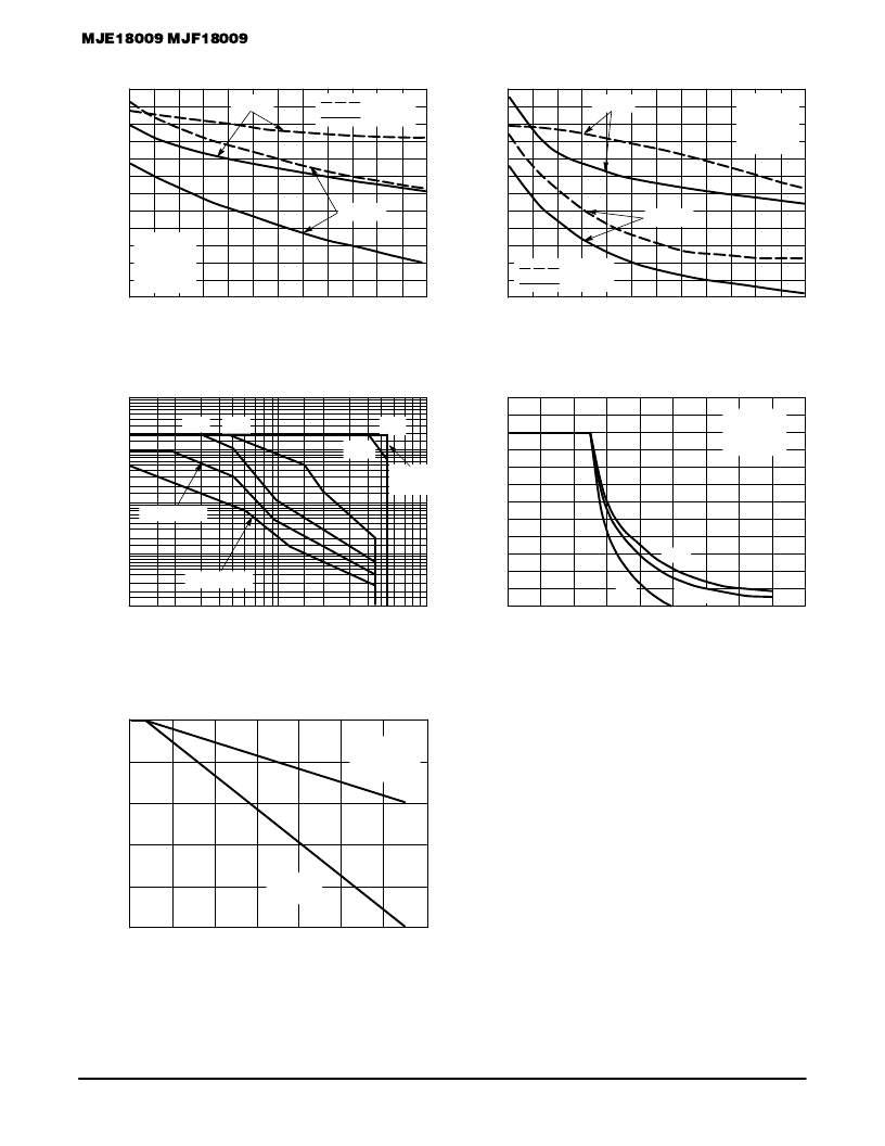
TYPICAL SWITCHING CHARACTERISTICS
Figure 13. Inductive Fall Time
160
40
15
7
3
hFE, FORCED GAIN
Figure 14. Inductive Crossover Time
400
200
100
15
5
3
hFE, FORCED GAIN
300
120
t
t
140
100
80
4
6
8
9
TJ = 125
°
C
TJ = 25
°
C
7
TJ = 125
°
C
TJ = 25
°
C
10
11
12
60
5
13
14
IBoff = IC/2
VCC = 15 V
VZ = 300 V
LC = 200
μ
H
IC = 3 A
IC = 6.5 A
9
11
13
IBoff = IC/2
VCC = 15 V
VZ = 300 V
LC = 200
μ
H
IC = 3 A
IC = 6.5 A
TYPICAL CHARACTERISTICS
Figure 15. Forward Bias Safe Operating Area
100
0.01
1000
10
VCE, COLLECTOR–EMITTER VOLTAGE (VOLTS)
Figure 16. Reverse Bias Switching Safe
Operating Area
12
4
0
1100
200
VCE, COLLECTOR–EMITTER VOLTAGE (VOLTS)
8
100
500
1
0.1
I
I
5 ms
1 ms
10
μ
s
1
μ
s
EXTENDED
SOA
0 V
–1.5 V
–5 V
TC
≤
125
°
C
GAIN
≥
4
LC = 500
μ
H
10
800
MJE18009–DC
MJF18009–DC
P
Figure 17. Forward Bias Power Derating
There are two limitations on the power handling ability of
a transistor: average junction temperature and second
breakdown. Safe operating area curves indicate IC–VCE
limits of the transistor that must be observed for reliable
operation; i.e., the transistor must not be subjected to
greater dissipation than the curves indicate. The data of
Figure 15 is based on TC = 25
°
C; TJ(pk) is variable
depending on power level. Second breakdown pulse limits
are valid for duty cycles to 10% but must be derated when
TC > 25
°
C. Second breakdown limitations do not derate the
same as thermal limitations. Allowable current at the
voltages shown on Figure 15 may be found at any case
temperature by using the appropriate curve on Figure 17.
TJ(pk) may be calculated from the data in Figures 20 and
21. At any case temperatures, thermal limitations will
reduce the power that can be handled to values less than
the limitations imposed by second breakdown. For induc-
tive loads, high voltage and current must be sustained
simultaneously during turn–off with the base–to–emitter
junction reverse biased. The safe level is specified as a
reverse–biased safe operating area (Figure 16). This rating
is verified under clamped conditions so that the device is
never subjected to an avalanche mode.
TC, CASE TEMPERATURE (
°
C)
1.0
0.8
0.6
0.4
0.2
0
160
140
120
100
80
60
40
20
SECOND
BREAKDOWN
DERATING
THERMAL
DERATING
相關(guān)PDF資料 |
PDF描述 |
|---|---|
| MJE18009 | POWER TRANSISTORS |
| MJE18009 | POWER TRANSISTORS 10 AMPERES 1000 VOLTS 50 and 150 WATTS |
| MJF18204 | POWER TRANSISTORS 5 AMPERES 1200 VOLTS 35 and 75 WATTS |
| MJF18204 | POWER TRANSISTORS |
| MJE18204 | POWER TRANSISTORS |
相關(guān)代理商/技術(shù)參數(shù) |
參數(shù)描述 |
|---|---|
| MJF18204 | 制造商:ON SEM 功能描述: 制造商:ON Semiconductor 功能描述: |
| MJF18206 | 制造商:ONSEMI 制造商全稱:ON Semiconductor 功能描述:POWER TRANSISTORS |
| MJF2955 | 功能描述:兩極晶體管 - BJT 10A 90V 30W PNP RoHS:否 制造商:STMicroelectronics 配置: 晶體管極性:PNP 集電極—基極電壓 VCBO: 集電極—發(fā)射極最大電壓 VCEO:- 40 V 發(fā)射極 - 基極電壓 VEBO:- 6 V 集電極—射極飽和電壓: 最大直流電集電極電流: 增益帶寬產(chǎn)品fT: 直流集電極/Base Gain hfe Min:100 A 最大工作溫度: 安裝風(fēng)格:SMD/SMT 封裝 / 箱體:PowerFLAT 2 x 2 |
| MJF2955G | 功能描述:兩極晶體管 - BJT 10A 90V 30W PNP RoHS:否 制造商:STMicroelectronics 配置: 晶體管極性:PNP 集電極—基極電壓 VCBO: 集電極—發(fā)射極最大電壓 VCEO:- 40 V 發(fā)射極 - 基極電壓 VEBO:- 6 V 集電極—射極飽和電壓: 最大直流電集電極電流: 增益帶寬產(chǎn)品fT: 直流集電極/Base Gain hfe Min:100 A 最大工作溫度: 安裝風(fēng)格:SMD/SMT 封裝 / 箱體:PowerFLAT 2 x 2 |
| MJF3055 | 功能描述:兩極晶體管 - BJT 10A 90V 30W NPN RoHS:否 制造商:STMicroelectronics 配置: 晶體管極性:PNP 集電極—基極電壓 VCBO: 集電極—發(fā)射極最大電壓 VCEO:- 40 V 發(fā)射極 - 基極電壓 VEBO:- 6 V 集電極—射極飽和電壓: 最大直流電集電極電流: 增益帶寬產(chǎn)品fT: 直流集電極/Base Gain hfe Min:100 A 最大工作溫度: 安裝風(fēng)格:SMD/SMT 封裝 / 箱體:PowerFLAT 2 x 2 |
發(fā)布緊急采購,3分鐘左右您將得到回復(fù)。